Why are designers moving away from traditional 2- or 4-layer PCBs—and increasingly embracing 2+N+2 stackups?
In modern PCB design, traditional 2-layer or 4-layer boards are increasingly reaching their practical limits—especially as today’s products demand higher component density, faster interfaces, and tighter electrical margins. While these simpler stackups still work for basic designs, they often struggle in more advanced applications.
Here’s where they commonly fall short:
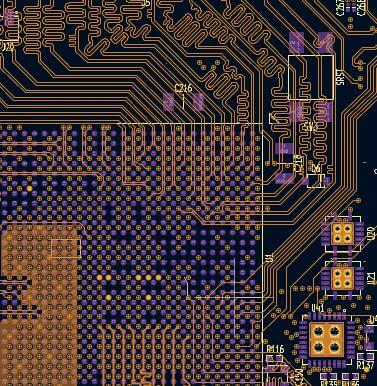
- BGA Fanout Limitations: Finer-pitch BGAs (for example, 0.5 mm pitch or below) are difficult—or sometimes impossible—to fully escape using only through-hole vias. This often leads to routing congestion, larger board outlines, or compromised layouts.
- High-Speed Routing Congestion: With limited signal layers, traces become overcrowded. This makes it challenging to maintain controlled impedance and clean return paths for high-speed interfaces such as DDR or PCIe.
- Poor Power Integrity: Inadequate or shared power and ground planes increase loop inductance, leading to voltage droop, noise, and unstable PDN behavior.
- EMI Challenges: Without proper layer referencing and shielding, designs are more susceptible to electromagnetic interference, increasing the risk of regulatory compliance issues.
To address these constraints, many designers are moving toward more advanced stackups such as 2+N+2—two outer build-up layers, an N-layer core, and two additional build-up layers. This approach introduces microvias for high-density interconnect (HDI)-like features, without the cost and complexity of a full HDI stackup.
The 2+N+2 architecture enables:
- Support for fine-pitch BGAs through efficient fanout using blind and buried microvias
- Higher routing density for compact and complex designs
- More reliable controlled-impedance routing for high-speed signals
- Improved power and ground referencing, resulting in lower noise and better overall PDN performance
Ultimately, 2+N+2 offers a balanced, cost-effective alternative to full HDI when higher density is required primarily on the outer layers. It delivers the electrical performance and routing flexibility demanded by modern electronics—while keeping manufacturing complexity and cost under control.
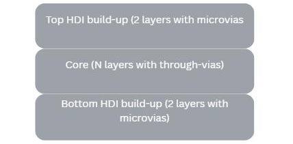
2+N+2 refers to a specific type of HDI PCB architecture that uses sequential lamination to combine a conventional multilayer core with HDI build-up layers on both sides.
The structure can be broken down as follows:
- The First “2”: Two build-up layers added to the top side of the core. These layers typically use laser-drilled microvias, finer trace geometries, and support higher routing density for component fanout and signal escape.
- “N” (The Core): A conventional multilayer sub-stack, where N represents the number of core layers. N is typically an even number (such as 4, 6, or 8) and is fabricated using mechanical drilling and plated through-hole vias.
- The Second “2”: Two additional build-up layers added to the bottom side of the core, again leveraging microvias and fine features to further increase routing flexibility.
Together, this configuration delivers many of the density and performance benefits associated with HDI designs—without fully committing to a more complex full-HDI stackup.
One of the defining characteristics of a 2+N+2 stackup is the way it is manufactured and how routing density is distributed across the board.
Sequential lamination is a key differentiator. Unlike standard multilayer PCBs—which are typically laminated in a single press cycle—a 2+N+2 board is built in stages. The core is fabricated first as a conventional multilayer board, including mechanical drilling, plating, lamination, and electrical testing. Once the core is complete, the top and bottom build-up layers are added through additional lamination cycles, with laser drilling used to form microvias between each stage.
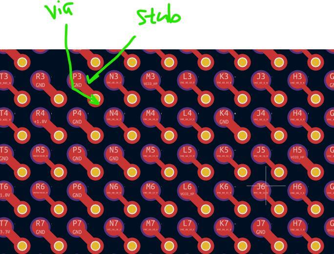
Another important distinction is where microvias are used. In a 2+N+2 design, microvias are confined to the build-up layers, typically as blind vias connecting the outer layers to the core. This allows for dense BGA fanout and fine geometries near the surface, while the core continues to rely on standard plated through-hole vias for deeper layer interconnection.
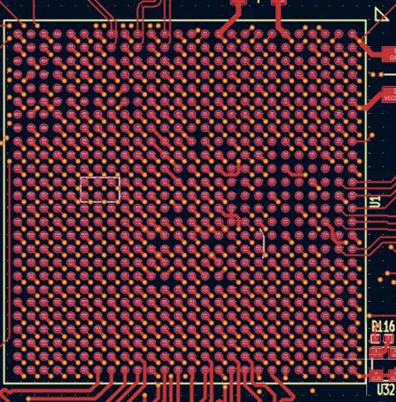
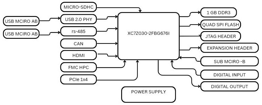
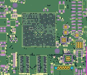
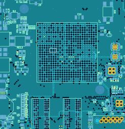
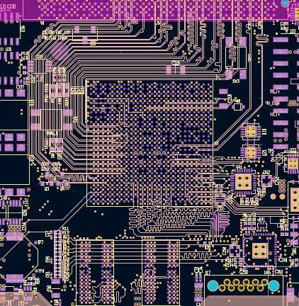
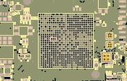
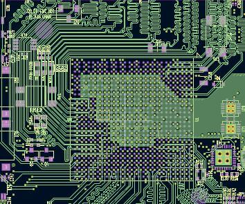
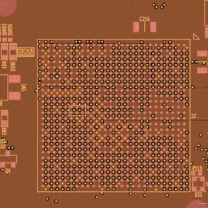
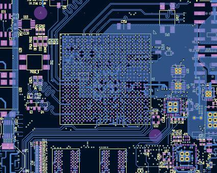
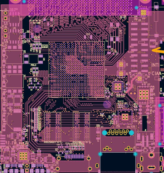
To illustrate why this matters, consider a design centered around the Xilinx Zynq XC7Z030 SoC. This device integrates a dual ARM Cortex-A9 processing system (PS) with 7-series FPGA fabric (PL) in a 676-pin BGA package.
Such a board requires:
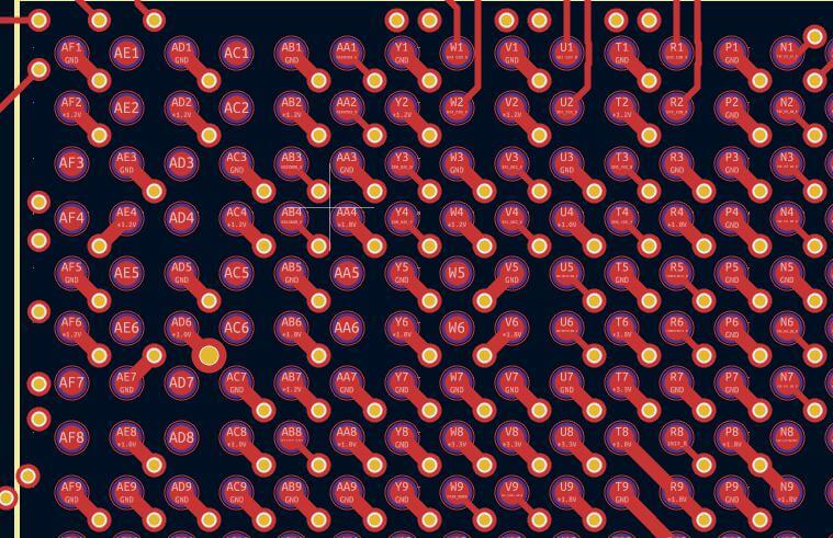
- Dense fanout to escape hundreds of BGA pins at a 1.0 mm pitch
- Controlled impedance routing for high-speed signals operating at several gigahertz, including DDR clocks, PCIe lanes (2.5–5 Gbps), and Ethernet interfaces
- Robust power distribution to minimize noise in mixed-signal regions shared by the PS and PL domains
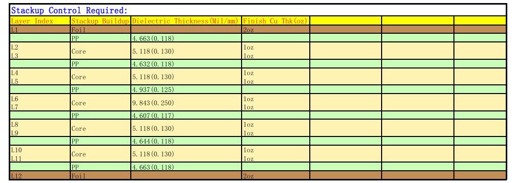
A simpler 4-layer stackup would quickly run into fanout and routing congestion issues under these constraints. By contrast, a 2+8+2 configuration provides the necessary routing density and electrical performance—without the added cost and complexity of a full HDI stackup.
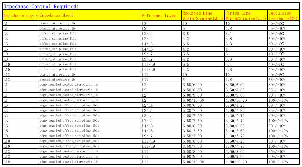
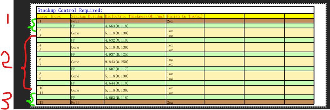
In this 2+8+2 stackup—with top build-up layers (L1–L2), a core stack (L3–L10), and bottom build-up layers (L11–L12)—the layer assignment is designed to balance signal integrity, power delivery, and EMI control.
- L1: Top Signal & Components
Component pads for BGAs and connectors, along with low-speed routing such as LEDs and control signals. Copper thickness is typically 1 oz, with heavier copper used only when mechanical durability or current requirements justify it.
Provides a continuous reference plane for L1 signals and supports blind microvias used for BGA fanout.
High-speed single-ended and differential routing, such as DDR address and control lines (typically targeting ~50 Ω single-ended impedance, depending on the stackup).
Dedicated reference plane for L3 to maintain controlled impedance and clean return paths.
Supplies I/O and peripheral rails with low DC resistance.
- L6: Ground Plane (Central Core)
A thicker core layer (approximately 0.25 mm) that improves board rigidity and provides low-inductance return paths across the stack.
Additional reference and shielding to help suppress EMI and reduce plane impedance.
Additional high-speed routing for dense interfaces that cannot be fully accommodated on L3.
Serves as a reference for L8 and further improves isolation between signal layers.
- L10: Inner Signal & Low-Voltage Power
Mixed-use layer supporting additional high-speed routing and a 1.0 V power plane for core logic rails.
Acts as the reference plane for L12 and supports bottom-side microvias.
- L12: Bottom Signal & Components
Secondary component placement and signal routing, typically used for lower-speed or space-constrained connections.
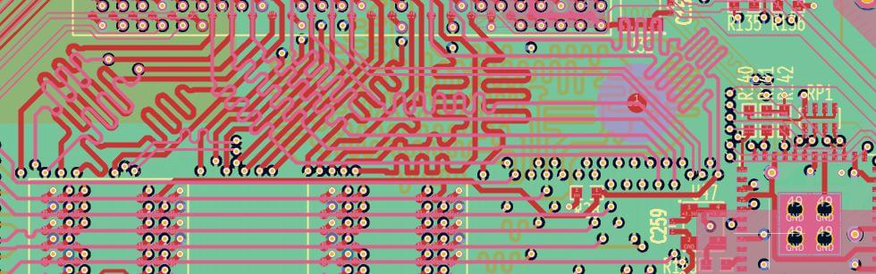
This is where 2+N+2 stackups truly shine. Routing in these HDI designs is not simply about adding more layers—it represents a strategic shift in how density, signal integrity, and manufacturability are managed.
Compared to traditional 2- or 4-layer boards (or even basic multilayer designs), where through-hole vias dominate and restrict BGA escapes, a 2+N+2 structure leverages microvias and fine features to enable segmented, purpose-driven routing without congestion.
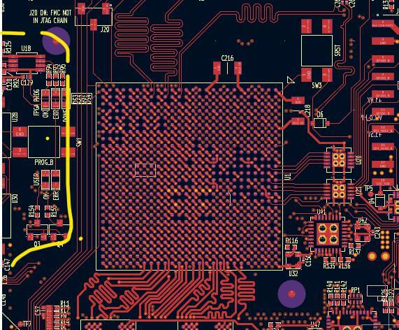
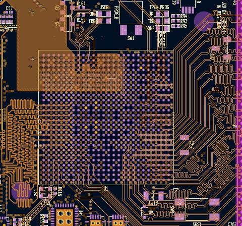
BGA fanout is almost always the primary routing bottleneck, so it should be addressed first.
In this design, outer ball rows escape directly on L1 or L12, while inner rows use blind microvias to transition to L2/L3 or L10/L11, avoiding vias that pass through the entire board. This “escape early” strategy clears valuable space beneath the BGA for decoupling capacitors, unlike standard designs where dense through-vias would force wider spacing and longer current loops.
The top and bottom build-up layers (L1–L2 and L11–L12) are optimized for this role. Microvias enable tight escapes with fine traces (for example, 4–6 mil geometries, depending on fabrication limits), allowing signals from Zynq I/Os or FMC connectors to fan out radially without overlap.
Critical interfaces—such as PCIe differential pairs or DDR clocks—benefit from being routed close to the surface. In this board, interfaces like USB or PCIe may route on L1 or L3, referenced to L2 ground, minimizing length mismatches and supporting controlled microstrip or stripline impedance (typically 85–100 Ω, depending on the interface).
The core layers (L3–L10) handle cross-board connections, such as FMC-to-Zynq PL banks or Ethernet traces. Stripline routing in these layers (for example, L5 referenced to L4/L6) provides better shielding and reduced EMI compared to long surface routes.
Power and ground planes on L4, L6, L7, and L9 distribute major rails (such as +1.0 V core and +3.3 V I/O) with low impedance. Dense via stitching supports high current demand—on the order of several amps—while avoiding the voltage drop and noise issues common in low-layer-count designs.
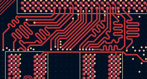
Fanout refers to how signals are routed away from BGA pads to traces and vias. In traditional multilayer boards, fanout options are typically limited to through-hole vias and relatively wide traces. A 2+N+2 stackup, however, enables more flexible and space-efficient fanout strategies.
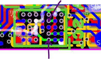
Dogbone fanout is a hybrid technique where a short breakout trace—the “bone”—connects the BGA pad to a nearby via pad. From there, a through-via or blind microvia transitions the signal to an inner layer.
In direct microvia fanout (Via-in-Pad), a filled and capped microvia is drilled directly into the BGA pad. This allows the signal to transition to another layer immediately, without consuming surface routing space. This method is especially effective for fine-pitch BGAs (typically below 0.5 mm), such as advanced SoCs, where traditional dogbone fanout would quickly run out of room.
Design for Manufacturing (DFM) ensures that your chosen 2+N+2 stackup aligns with the actual capabilities of your PCB fabricator. Ignoring DFM considerations can lead to microvia reliability issues, poor plating quality, and latent failures—especially under thermal cycling in industrial or long-life applications.
Before finalizing a 2+N+2 design, it is critical to confirm the following parameters with your fabrication partner:
This includes the laser drill diameter (typically 0.10–0.15 mm, or 4–6 mil) and the aspect ratio (depth-to-diameter). For reliable copper plating, an aspect ratio of < 0.75:1 is generally recommended to avoid voids and weak barrel formation.
- Maximum Number of Sequential Laminations:
Many fabricators limit HDI builds to 3–4 total lamination cycles to control warpage and layer-to-layer registration accuracy. Exceeding this range often requires premium processes and significantly increases cost.
- Allowed Microvia Stacking Strategy (Stacked vs. Staggered):
Stacked microvias—where vias are directly aligned—offer higher density but can become reliability risks when stacked more than 2–3 layers due to concentrated mechanical stress.
Staggered microvias, typically offset by 0.075–0.10 mm, distribute stress more evenly and generally provide better long-term reliability.
It’s also important to recognize that HDI is not inexpensive. A 2+N+2 board can cost roughly 2–5× more than a basic multilayer PCB, driven by additional lamination cycles, laser drilling, and tighter process controls.
We’ve explored the fundamentals of 2+N+2 stackups—from why traditional boards fall short to what actually defines a true 2+N+2 structure. As you’ve seen, this approach is not just “adding more layers,” but making intentional design choices to manage density, signal integrity, and manufacturability.
Key Rules to Remember:
- Always escape BGAs first, using microvias—whether dogbone or via-in-pad—to avoid routing deadlocks later.
- Leverage the outer HDI layers for fanout and short high-speed paths, and reserve the inner core layers for long routes and solid planes.
- Engage your PCB fabricator early to confirm microvia limits, stacking rules, and fine-feature capabilities.
- Simulate impedance and PDN behavior—don’t rely on assumptions.
- Prioritize symmetry and DFM to minimize warpage, yield loss, and long-term reliability risks.
Ultimately, designing 2+N+2 PCBs is less about layer count and more about controlling geometry, current paths, and manufacturing realities.
If you’re ready to turn a 2+N+2 design into hardware, PCBCool works with engineers to validate stackups, microvia strategies, and DFM constraints before fabrication begins. By aligning design intent with real manufacturing capability, we help ensure that advanced HDI designs build reliably the first time—without unnecessary cost or iteration.