Microvias are small laser-drilled interconnects used in high-density interconnect (HDI) PCB. They allow signals to move between closely spaced layers without using the larger space required by traditional through-hole vias. This makes them especially useful in compact PCB designs where fine-pitch components, dense routing, and limited board area must be managed at the same time.
However, a microvia is not simply a smaller version of a standard via. Its performance depends on whether the via structure can be reliably drilled, plated, filled, laminated, and assembled. A design that looks correct in the PCB layout may still create manufacturing or reliability risks if the aspect ratio, capture pad, copper filling, or lamination process is not properly controlled.
This is why microvia design rules are important in HDI PCB manufacturing. They help designers and manufacturers define practical limits for geometry, process control, and long-term reliability before the board enters production. In this article, we will explain the key design and manufacturing factors that affect microvia quality, reliability, and manufacturability in HDI PCB.
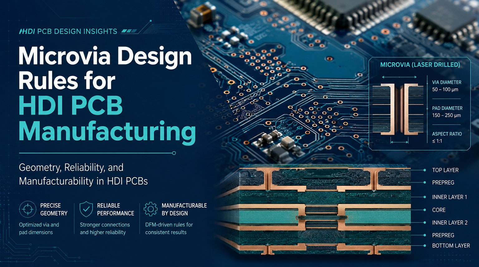
Microvia design rules define the manufacturing specifications of laser-drilled interconnects in HDI PCB, both geometrically and electrically. These rules specify limits for aspect ratio, capture pad size, copper fill, layer sequencing during lamination, and thermal reliability under cyclic loading conditions.
According to IPC-based design guidance for microvias used primarily in HDI builds, the hole diameter is generally limited to less than 150 µm.
Microvias should have a maximum aspect ratio of 0.75, measured from the dielectric thickness to the final finished diameter of the microvia. This helps produce good copper termination and avoid voids when the microvia cavity is filled with copper.
A typical example is a 100 µm finished microvia with a maximum allowable dielectric thickness of 75 µm. If this ratio is exceeded, non-uniform plating may occur around the knee of the microvia, and copper deposition on the capture pad interface may be reduced.
Capture pad diameters for 100 µm laser microvias are commonly designed up to 300 µm to allow for a sufficient annular ring based on ±25 µm of layer-to-layer tolerance.
For a sufficient annular ring, IPC-2226 also specifies minimum target pad coverage on capture pads to accommodate UV laser positional drift and dielectric shrinkage during each consecutive lamination cycle.
Microvia geometry must also consider resin flow during lamination. Taper angles of 5° to 15° are used to improve copper throwing power and reduce trapped chemistry during electroplating. Flat-bottom via profiles are avoided because they can create localized stress concentration under thermal cycling conditions.
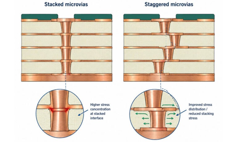
When constructing multilayer HDI structures that use stacked or staggered microvias, the primary manufacturing process is sequential lamination. Each build-up layer is separately fabricated through multiple sequential processes, including lamination, laser drilling, metallization, and imaging.
According to IPC-2226, cumulative z-axis registration errors become significantly larger beyond two sequential stacks. Therefore, each drill cycle should create only one microvia layer within each stacked microvia structure.
Core thickness selection directly affects lamination stability and registration accuracy. HDI cores are manufactured with a thickness of 100 to 400 µm, while dielectric build-up layers are generally produced using resin-coated copper (RCC) dielectrics with a thickness of 50 to 75 µm to maintain practical aspect ratios.
The dielectric thickness distribution within a stack should remain uniform. If it is not uniform, the material can expand at different rates during thermal lamination due to non-uniform resin distribution.
Lamination temperatures usually range from 170°C to 190°C, depending on the Tg characteristics of the resin system used. Registration tolerances after sequential lamination can be achieved within ±30 µm by using an X-ray optical alignment system.
Poor stack symmetry or excessive build-up count can lead to warpage and directly affect capture pad alignment accuracy during laser drilling operations.
The quality of microvia metallization depends mainly on:
- Uniformity of copper fill
- Plating thickness distribution
- Void-free copper deposition along the via barrel and capture interface
To achieve a full copper fill without a center void in HDI manufacturing, pulse electroplating or intermittent reverse-pulse plating is commonly used.
IPC-6016 specifies the minimum copper plating thickness required for HDI structures. This is based on maintaining a copper thickness of 25 µm in the knee region of the microvia. However, local thickness variation in plated copper should be kept to a minimum. If too much copper builds up around the via opening, over-plating stress may increase and create a crack risk during thermal cycling.
The copper caps above filled microvias typically vary from 8 to 15 µm to maintain a flat surface geometry for future build-up lamination processes. Poor planarization of these copper caps can produce resin erosion and unbalanced dielectric thickness in the upper layers.
In a stacked microvia structure, void acceptance limits are extremely low. Even very small voids below 10 µm near the capture pad interface can deteriorate under repeated thermal cycling between -40°C and 125°C during IPC reliability qualification testing.
The reliability of stacked microvias is largely dictated by the accumulation of stress at the interface between the microvia and its target pad during temperature cycling. Most of the strain builds up in the knee region of the microvia, where copper plating transitions from the barrel to the target pad.
Finite element analysis shows that when the vertical height of stacked microvias exceeds two stacked microvias, stress intensity becomes significantly greater. This is mainly due to cumulative misalignment and the difference in z-axis expansion between copper and the surrounding dielectric material.
The fatigue life of copper is also affected by the copper grain structure formed during electroplating. Fine equiaxed grains produced through reverse-pulse electroplating have a lower crack propagation rate than columnar grain structures produced by conventional DC electroplating.
Grain boundary failure becomes increasingly critical during thermal cycling between -40°C and +125°C, especially in automotive and aerospace HDI applications.
Propagating corner cracks generally occur in microvias where localized plating thickness is less than 15 µm. As thermal expansion and contraction cycles increase, crack propagation continues within the copper interface until complete failure occurs.
Microvia escape routing density is restricted by several design parameters, including BGA pitch, capture pad dimensions, escape trace width, and total PCB build-up layer count.
For a 0.5 mm BGA pitch, common escape strategies use laser-drilled microvias up to 100 µm and capture pads up to 250 µm. Microvias are copper-filled and planarized to help prevent solder voids and paste wicking during BGA assembly.
However, copper-filled microvias located directly below solder pads can also create inconsistent solder joint volumes during reflow, which may introduce reliability concerns.
Escape channel geometries are calculated based on solder mask registration tolerances. Using a 0.4 mm pitch BGA and 200 µm diameter capture pads, around 100 µm routing clearance would exist between a pair of pads before any solder mask expansion is applied.
As a result, many advanced HDI designs require modified semi-additive manufacturing processes to provide escape routing with less than 40 µm line widths between inner rows without significantly increasing the number of layers.
Microvia transitions can introduce localized impedance discontinuities. These discontinuities are caused by abrupt changes in current distribution, differences in reference plane geometry, and uneven parasitic capacitance from one side of the via interface to the other.
At gigahertz frequencies and above, even very short microvia transitions can create insertion loss and mode conversion if return path continuity is not maintained at the layer-to-layer transition.
Blind microvias usually have shorter stub lengths than through-hole vias, reducing the resonant behavior caused by stub inductance. This resonance occurs as the stub length approaches one-quarter wavelength of the signal’s rise-time frequency.
For example, if the residual blind microvia stub length exceeds 300 µm, it can affect the total reflected impedance of the microvia above 10 GHz, depending on dielectric constant and propagation velocity.
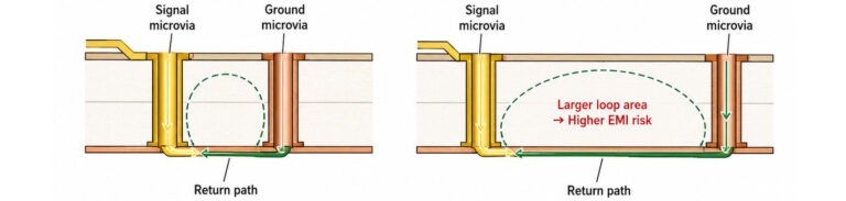
To maintain electrical signal integrity between microvia layers, the grounding return structure must provide adequate coupling. This minimizes loop inductance and helps preserve electromagnetic coupling between the microvia signal transition and the microvia reference plane transition.
The ground microvia is typically placed 250 to 500 µm from the high-speed signal microvia. Increased spacing between the signal and reference plane transitions will increase loop area, increase localized electromagnetic emissions, and create differential impedance imbalance.
Capture pad diameter also influences parasitic capacitance around the microvia barrel. A larger capture pad diameter generates more parasitic capacitance, which can produce localized impedance dips near the microvia barrel and reduce high-speed channel uniformity when routed near multiple HDI traces.
Laser drilling accuracy has a direct impact on how many microvias can be accommodated, how reliable capture pads are, and how accurately interlayer registration is formed.
With UV lasers, positional tolerance can reach ±20 µm. CO₂ laser systems have slightly larger positional tolerance due to their higher thermal effect on the dielectric. In fine-pitch designs, if the capture pad diameter is less than 225 µm, registration error becomes critical.
Cumulative tolerances determine how capture pads should be fabricated. These tolerances include lamination-induced shrinkage, imaging offsets, drill alignment variation, and differences in the coefficients of thermal expansion between materials.
If the finished position tolerance of a microvia is ±20 µm and the finished microvia diameter is 100 µm, the capture pad diameter should be 250 µm to provide adequate annular coverage after lamination.
Another concern is the accuracy of dielectric removal at the bottom of the via. If excessive laser energy is used, the copper foil can be damaged or thermally degraded under the dielectric. This can prevent a strong metallurgical bond and weaken the interconnect.
The main limiting factors for HDI manufacturability are laser drill tolerance, copper filling uniformity, and accurate sequential lamination. In most manufacturing processes, microvias use a minimum diameter between 75 µm and 100 µm, while capture pads must be larger than 225 µm to maintain acceptable yield.
A high density of microvias contributes to cumulative positioning errors across lamination layers, especially in stacked microvia structures.
From an assembly standpoint, fine-pitch BGAs often use via-in-pad design. These microvias must be filled with copper and planarized before soldering so that copper does not wick solder away from the solder joint during reflow.
Inadequately filled microvias can reduce solder joint volume and increase the probability of head-in-pillow defects. Resin loss around capped microvias can also create localized stress concentration during thermal cycling.
Inspection capability is another constraint. HDI density is restricted by the ability of AOI systems to reliably inspect traces and vias under 50 µm. In most cases, voids inside microvias can only be detected by X-ray inspection or destructive cross-sectional analysis.
Microvias allow HDI PCB to support finer routing, higher interconnect density, and more compact package escape. However, their reliability depends on much more than hole size. The via geometry, copper filling, plating quality, lamination sequence, and registration accuracy must all be realistic for the manufacturing process.
For engineers working on fine-pitch BGA, high-speed, or other advanced HDI applications, early manufacturability review is essential. A microvia structure that works in layout must also be suitable for laser drilling, copper filling, sequential lamination, inspection, assembly, and long-term thermal reliability.
PCBCool supports HDI PCB projects from early design review to fabrication and assembly. If your project involves stacked microvias, via-in-pad structures, fine-pitch BGA escape routing, or high-reliability HDI requirements, our team can help evaluate manufacturability risks before production and provide practical manufacturing support.