Industrial PCB design is a different discipline from standard consumer electronics design. In this space, the goal is not simply to make a board function at the lowest possible cost or move quickly from prototype to production. The real challenge is building hardware that can operate reliably for years in harsh, unpredictable environments.
That means industrial PCBs must be designed with far tighter attention to reliability, durability, and long-term stability. They often need to withstand vibration, wide temperature swings, humidity, dust, chemical exposure, electrical noise, and extended service lives that can stretch well beyond a decade. On top of that, they must meet stricter safety and compliance requirements while remaining practical for repeatable, high-volume manufacturing with low field-failure risk.
This article assumes familiarity with standard PCB design fundamentals such as layout rules, trace sizing, and manufacturing outputs. The focus here is on what changes when a board is expected to survive real industrial conditions rather than a controlled consumer environment.
Industrial PCBs are engineered to endure demanding environments far beyond typical consumer applications, such as factories, outdoor installations, or heavy machinery. This involves designing for extremes in temperature, mechanical stress, moisture, and contaminants to ensure reliability, longevity, and safety. Key considerations include material choices, layout optimizations, protective coatings, and rigorous testing. Below, we’ll dive deeper into each aspect, including practical strategies, tools, and best practices drawn from industry standards.
In industrial settings, PCBs may face temperatures ranging from -40°C to +125°C or higher, where poor heat handling can lead to component failure, reduced lifespan, or system shutdowns. Effective thermal management focuses on dissipating heat from high-power components like processors, power transistors, or LEDs while maintaining operational stability.
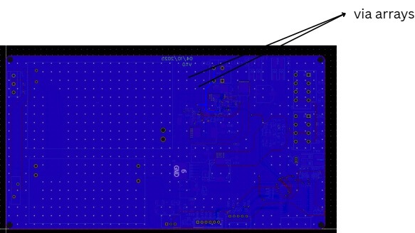
This creates low-resistance paths for heat transfer from surface layers to inner copper planes or the opposite side of the board. These are plated through-holes filled or tented to conduct heat vertically.
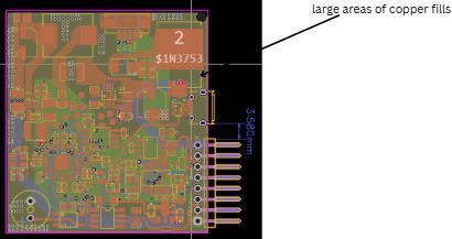
Large areas of copper fill on the PCB—act as heat spreaders, distributing thermal energy across the board to prevent hotspots.
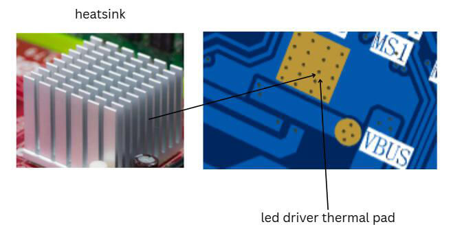
Directly onto components or via thermal pads for enhanced convection or radiation. For high-performance designs, consider metal-core PCBs (MCPCBs) with aluminum or copper substrates for superior conductivity.
Derate components by operating them below their maximum ratings—e.g., reduce current through resistors by 50% in hot environments to account for increased resistance and aging. Select industrial-grade parts with wider temperature ranges, like capacitors rated for -55°C to +150°C. Low temperatures can cause brittleness, so use flexible solders or underfills to prevent cracks.
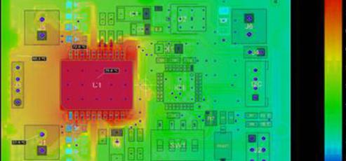
Employ software like Ansys Icepak, Autodesk CFD, or Altium’s built-in thermal analyzer for simulations. These tools model heat flow, identify hotspots, and optimize layouts before prototyping. Input parameters include component power dissipation, ambient conditions, and material properties for accurate predictions.
Industrial PCBs in vehicles, machinery, or seismic zones must withstand vibrations (e.g., 5-2000 Hz) and shocks (up to 100g), which can cause solder joint fatigue, component detachment, or trace cracks. Design emphasizes mechanical integrity through securing methods and analysis.
- Component securing techniques
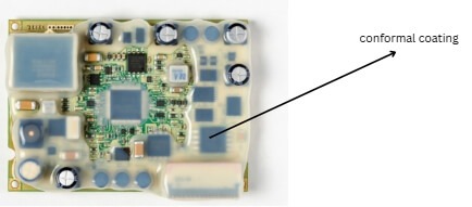
Apply conformal coatings—thin polymeric layers (acrylic, silicone, urethane)—to dampen vibrations and hold components in place. Potting encases the entire board in epoxy or silicone for ultimate protection, absorbing shocks but adding weight. Use staking or adhesives for tall components, and edge-bonding for BGAs to reinforce solder balls.
- Selection of flexible or rigid
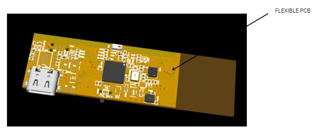
Rigid FR-4 boards suit most applications, but flexible polyimide or hybrid rigid-flex PCBs absorb vibrations better in dynamic environments like automotive or aerospace. Increase board thickness (e.g., 2-3mm) to raise resonant frequency, ideally 3x higher than the shock pulse frequency to avoid amplification.
- FEA for mechanical stress
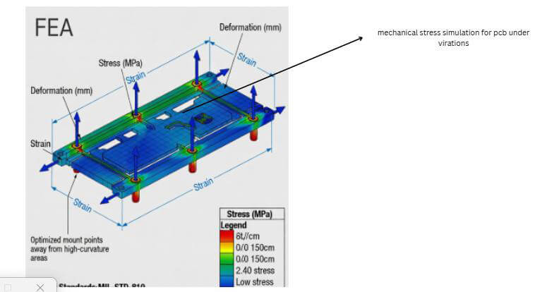
Finite Element Analysis (FEA) tools like Ansys Mechanical or SolidWorks simulate stress, strain, and deformation under vibration. Model the PCB as a beam or plate, input modal frequencies, and optimize mount points (e.g., place them away from high-curvature areas). Testing follows standards like MIL-STD-810 for random vibration or IEC 60068 for shock.
High humidity (up to 95% RH) and corrosive elements like salts or pollutants can lead to dendritic growth, shorts, or metal oxidation on PCBs. Protection strategies focus on barriers and material resilience.
Use enclosures rated IP65 or higher to seal against water ingress. Materials like polycarbonate or stainless steel provide robust housing, with gaskets ensuring tight fits.
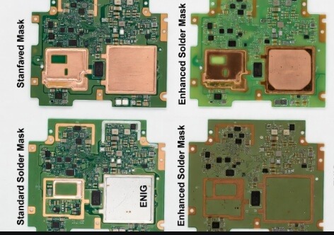
Standard solder masks offer basic protection; enhance with thicker layers or specialized masks (e.g., liquid photoimageable) for better coverage. Avoid exposed copper by using finishes like ENIG (Electroless Nickel Immersion Gold) or OSP (Organic Solderability Preservative) to resist oxidation.
Replace standard FR-4 with polyimide or PTFE-based substrates for high-humidity tolerance, as they have low moisture absorption (under 0.1%). For extreme corrosion, use halogen-free laminates. Control storage and assembly humidity (40-60% RH) to prevent pre-assembly issues.
Dust accumulation can cause overheating, while chemicals (acids, solvents) erode materials. Industrial designs incorporate barriers and testing to maintain functionality in contaminated environments.
Conformal coatings or potting create seals against dust and mild chemicals. For harsher exposures, use parylene coatings for their superior chemical resistance and thin profile (2-50 microns).
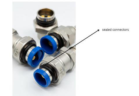
Employ IP67-rated connectors with rubber seals or O-rings to prevent ingress at interfaces. Hermetic seals (glass-to-metal) are ideal for extreme chemical environments.
Conduct salt spray tests (ASTM B117) to simulate corrosive atmospheres, or chemical immersion per IPC-TM-650. Use HEPA-filtered vacuums for cleaning during abatement or maintenance to avoid spreading contaminants. For chemical resistance, select coatings like silicone for flexibility or urethane for abrasion resistance
Industrial PCBs frequently operate in electrically noisy settings—near motors, inverters, relays, welders, variable frequency drives (VFDs), or heavy machinery—where electromagnetic interference (EMI) is severe and power quality fluctuates. Maintaining signal integrity (SI) ensures clean, undistorted high-speed signals reach their destinations without bit errors, while power integrity (PI) guarantees stable voltage rails despite transient demands and noise. Poor SI/PI leads to intermittent failures, false triggering, data corruption, or complete system downtime—unacceptable in industrial control, automation, robotics, or process monitoring.
EMI/EMC compliance (e.g., IEC 61000 series, CISPR standards) is critical. Industrial environments demand designs that both emit low EMI and resist high external interference (immunity).
- Grounding and reference planes
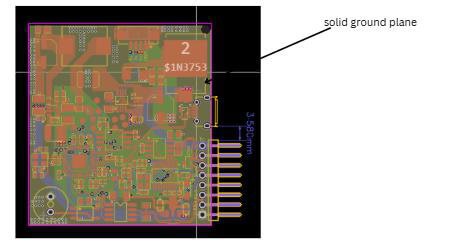
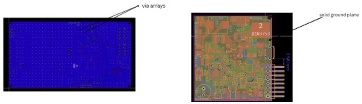
Use solid, unbroken ground planes (avoid splits under high-speed signals). Implement via stitching every few mm along plane edges and transitions to maintain low-impedance return paths and suppress common-mode currents.
Apply metal cans or shields over sensitive sections (e.g., analog, RF, or high-speed digital). Use EMI gaskets and dense ground vias around shield perimeters.
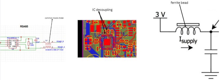
Place common-mode chokes, ferrite beads on power/clock lines, and π-filters (cap-inductor-cap) at interfaces. Use TVS diodes or MOVs for surge protection.
- Layer stackup optimization
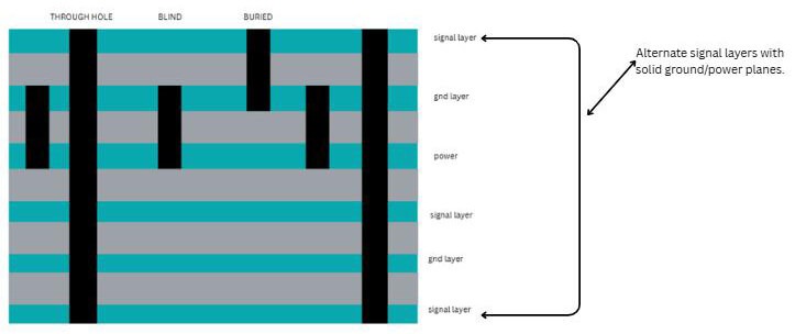
Alternate signal layers with solid ground/power planes. Route critical signals on inner layers sandwiched between planes for natural shielding.
Physically separate noisy (power switching, relays) from sensitive (analog, high-speed serial) sections. Use moats or guard traces if needed.
The Power Distribution Network (PDN) must deliver low-impedance power with minimal voltage droop, ripple, or noise under dynamic loads.
Place low-ESR ceramic capacitors (0.1 µF–10 µF) as close as possible to IC power pins. Use via-in-pad or blind vias for shortest paths. Combine bulk (electrolytic/tantalum) with high-frequency decoupling.
Dedicate wide copper pours or full planes for power and ground. Use multiple vias in grids to connect planes across layers, reducing inductance.
Aim for PDN impedance below 10–50 mΩ in the frequency range of interest (DC to GHz). Simulate with tools like HyperLynx, SiWave, or Ansys SIwave to identify anti-resonances.
Stitch power/ground planes densely to minimize loop inductance.
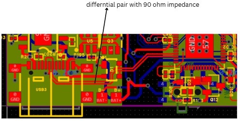
For signals >100 Mbps (e.g., Ethernet, CAN FD, PCIe, LVDS, SerDes), treat traces as transmission lines.
Route differential pairs (100 Ω) or single-ended (50 Ω) with consistent width/spacing. Use field solvers in PCB tools (Altium, Cadence) to calculate stackup.
Keep length-matched pairs, minimize vias/stubs, avoid sharp bends (>45° preferred). Route over solid reference planes.
Industrial PCBs are often produced in medium to high volumes (thousands to tens/hundreds of thousands of units) for applications like automation controllers, motor drives, sensors, or SCADA systems. Success depends on designing for efficient, repeatable manufacturing while minimizing defects, costs, and lead times. This involves Design for Manufacturability (DFM), Design for Testability (DFT), robust supply chain strategies, assembly optimizations for scale, and continuous yield improvement.
Early collaboration with your PCB fabricator and assembly house (CM/EMS) is essential—share your target volumes, get their DFM/DFA guidelines, and run manufacturability checks during layout.
DFM optimizes the bare board and assembly for fabrication and placement to reduce defects, scrap, and rework. DFT ensures the board can be quickly and thoroughly tested post-assembly to catch issues early.
- Penalization for efficiency
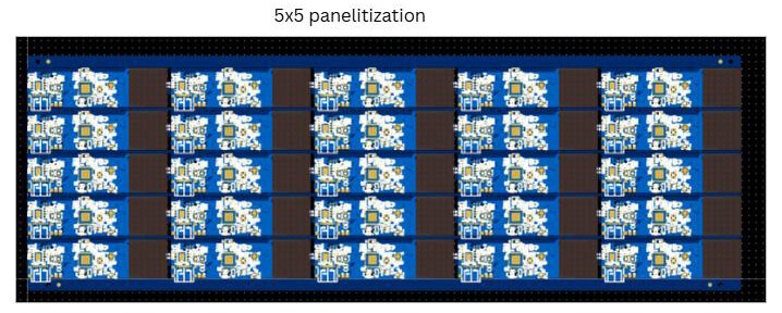
Group multiple PCBs on larger panels (e.g., 18×24 in or custom) to maximize material use and automate handling. Include fiducials (global and local) for precise machine alignment, tooling holes for fixturing, and rails (0.5–1 in wide) for conveyor transport. Choose depanelization method: V-scoring for straight edges (low cost, high stress) or tab routing with mouse bites (flexible shapes, lower edge stress).
Use standard packages (0603/0805 passives preferred over 0402 for reliability in industrial vibration/thermal cycling). Maintain minimum trace width/spacing (e.g., 6 mil/6 mil typical), annular ring ≥0.15 mm, and solder mask dam ≥0.1 mm. Avoid via-in-pad unless filled/capped; prefer tented vias. Add teardrops at trace-pad junctions to prevent breakout during etching.
- Testability features (DFT)
Include dedicated test points (≥1 mm diameter pads) on every net, especially power, ground, and critical signals. Place them in a grid for bed-of-nails ICT (in-circuit test) or accessible for flying probe. Add boundary scan (JTAG) chains for complex digital designs. Prioritize high-risk nets (e.g., fine-pitch BGAs) early in schematic phase.
Industrial electronics face long product lifecycles (10–20+ years), making obsolescence and shortages major risks (e.g., post-2020 chip crisis lessons).
- Multi-sourcing & alternatives
Specify second-source options in BOM (e.g., multiple MCU families). Use centralized libraries with alternate parts flagged.
Lock in components early for high-volume runs; use consignment or vendor-managed inventory (VMI) for critical items.
Avoid single-region dependency (e.g., mix Asia, Europe, domestic). Qualify multiple fabs/CMs for risk mitigation.
Track lifecycle status via tools like SiliconExpert or IHS; design in drop-in replacements where feasible.
Include isolation, redundancy, and wide-temp parts to reduce field failures that trigger urgent re-sourcing.
High-volume (>10,000 units/run) shifts to full automation: SMT lines with high-speed pick-and-place (30,000–100,000 CPH), precise stencil printing, reflow ovens, and inline inspection.
Fine-tune stencil thickness/aperture for consistent paste volume. Use nitrogen reflow for Pb-free reliability. Integrate AOI at multiple stages (post-paste, pre-reflow, post-reflow) for defect detection.
Industrial PCBs must prioritize human safety, equipment protection, and regulatory approval to prevent electrical hazards like shock, fire, arc flash, or explosions—especially in environments with high voltages, harsh conditions, or explosive atmospheres. Compliance involves designing for proper insulation, spacing, and isolation while navigating a maze of international and regional standards. Key areas include creepage and clearance distances, galvanic isolation techniques, hazardous location rules, and certification processes.
Non-compliance can lead to failed certifications, product recalls, liability issues, or catastrophic failures in the field.
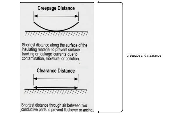
These are the two fundamental spacing rules that prevent arcing, tracking, or breakdown between conductors at different potentials.
- Clearance: The shortest distance through air between two conductive parts (prevents flashover/arcing in air).
- Creepage: The shortest distance along the surface of the insulating material (prevents surface tracking or leakage currents due to contamination, moisture, or pollution).
Requirements depend on:
- Working voltage (peak or RMS)
- Pollution degree (PD): PD1 (clean), PD2 (typical office/industrial), PD3 (industrial with conductive pollution), PD4 (severe outdoor)
- Material group (CTI—Comparative Tracking Index): I (best, ≥600), II (400–600), IIIa/IIIb (worst, <400; FR-4 often IIIa/b)
- Insulation level: Functional (operation only), Basic (shock protection), Supplementary, Reinforced/Double (highest safety, e.g., for user-accessible parts)
- Altitude (reduced air density above ~2000 m requires derating)
- Coating (conformal coating can reduce requirements in some standards)
Key Standards:
- IPC-2221B: Generic PCB design guideline; provides baseline tables for clearance/creepage (often used early in design).
- IEC 60664-1: Foundational for insulation coordination in low-voltage systems (<1000 V AC / 1500 V DC); defines pollution degrees and tables.
- IEC 62368-1: Modern hazard-based safety standard (replaced IEC 60950-1 for AV/IT equipment); widely adopted for reinforced isolation.
- IEC 60950-1 (legacy, but still referenced): For IT equipment.
- UL 60950-1 / UL 62368-1: US harmonized versions; often required for North American markets.
- Others: IEC 61010-1 (measurement/control/lab equipment), UL 508 (industrial control).
Galvanic isolation prevents direct current flow between circuits (e.g., control side vs. power side) while allowing signal/power transfer—critical for safety in industrial systems with mixed voltages.
Common Methods:
- Optocouplers: Optical (LED + phototransistor); simple, low-cost for signals; good for digital I/O, feedback loops.
- Transformers: Inductive; excellent for power (isolated DC-DC converters) and AC signals; supports voltage step-up/down.
- Capacitive Isolators: Use high-voltage capacitors; modern digital isolators (e.g., SiO₂ barrier) offer high speed, low power, excellent CMTI (common-mode transient immunity >100 V/ns).
- Magnetic Isolators: Inductive coupling in ICs; similar to transformers but integrated.
Standards:
- IEC 60747-5-5 (optocouplers)
- IEC 60747-17 (capacitive/magnetic isolators)
- Require reinforced isolation for safety-critical paths (e.g., 5–10 kV surge withstand).
Implementation Tips:
- Place isolation barrier midway; minimize crossings.
- Use wide-body packages (e.g., SOIC-16 WB) for higher creepage (7–8 mm).
- Ensure CMTI matches switching transients (e.g., SiC/GaN drivers).
- Combine with isolated power supplies for full barrier.
- Identify end-use (industrial control? Hazardous area? Medical?).
- Select primary standard (e.g., IEC 62368-1 for general industrial).
- Calculate creepage/clearance early (use tools/tables).
- Implement isolation where needed (reinforced for user safety).
- Prototype and test (hi-pot, partial discharge, insulation resistance).
- Engage certification body (UL, TÜV, CSA, SGS) for pre-compliance.
- Document everything (risk assessment, rationale).
- For hazardous: Add Ex protection and certify via IECEx/ATEX.
Industrial PCB design is less about achieving the highest performance on paper and more about delivering boring, predictable, long-term reliability in ugly real-world conditions. When your board keeps running flawlessly inside a steel mill, on an offshore platform, or in a 24/7 automated factory for a decade or more — that is the true measure of success.
At PCBCool, we provide complete EMS services, covering industrial PCB manufacturing, PCB assembly, and full project support for a wide range of industrial applications. If you are facing challenges in industrial PCB design, manufacturing, or assembly, our team is ready to help. From prototype evaluation to production execution, we can support you with a more complete and practical solution for your industrial PCB project.