


Tag Archives: High-Density Interconnect
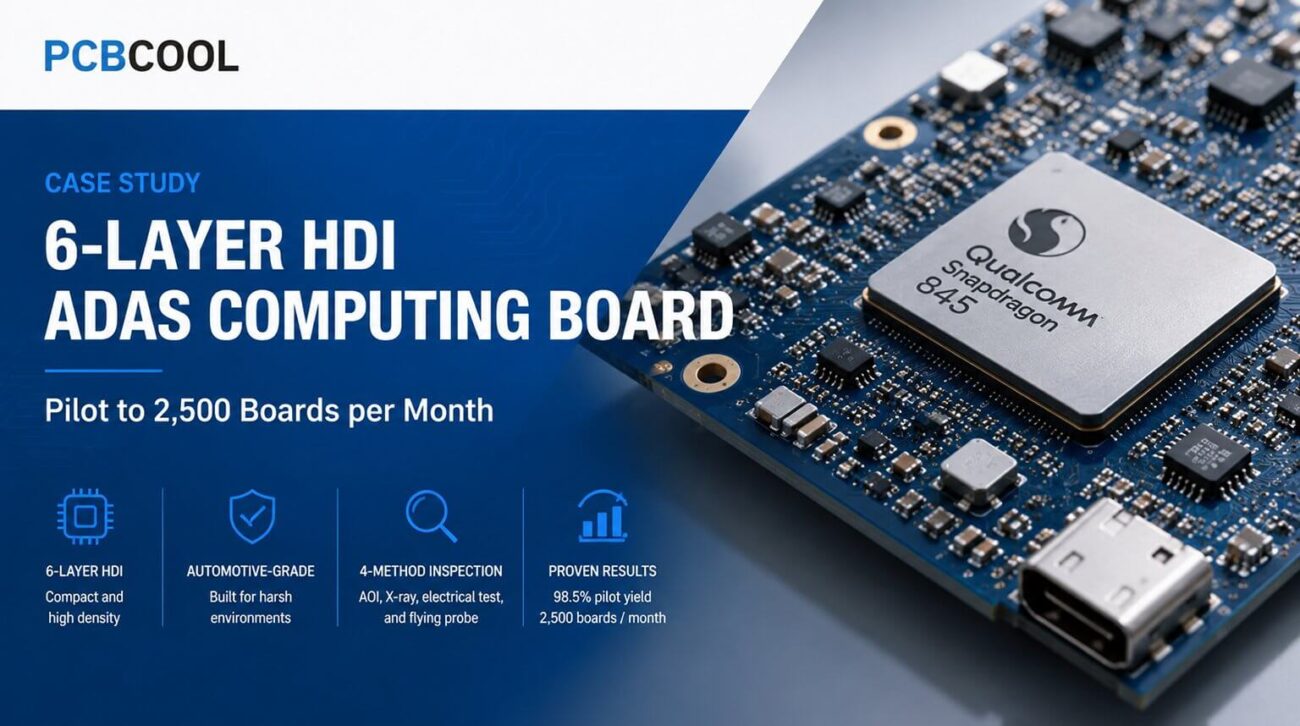
6-Layer HDI ADAS Computing Board PCB Case Study
See how PS Electronics helped an ADAS customer solve a mid-volume HDI PCB manufacturing challenge, achieving 98.5% pilot yield and 2,500 boards per month.
Sequential Build-Up (SBU) Manufacturing Technology in HDI PCB
Learn about Sequential Build-Up (SBU) technology in HDI PCB manufacturing, including layer-by-layer fabrication, microvia reliability, common challenges, and best practices for improving yield and performance.
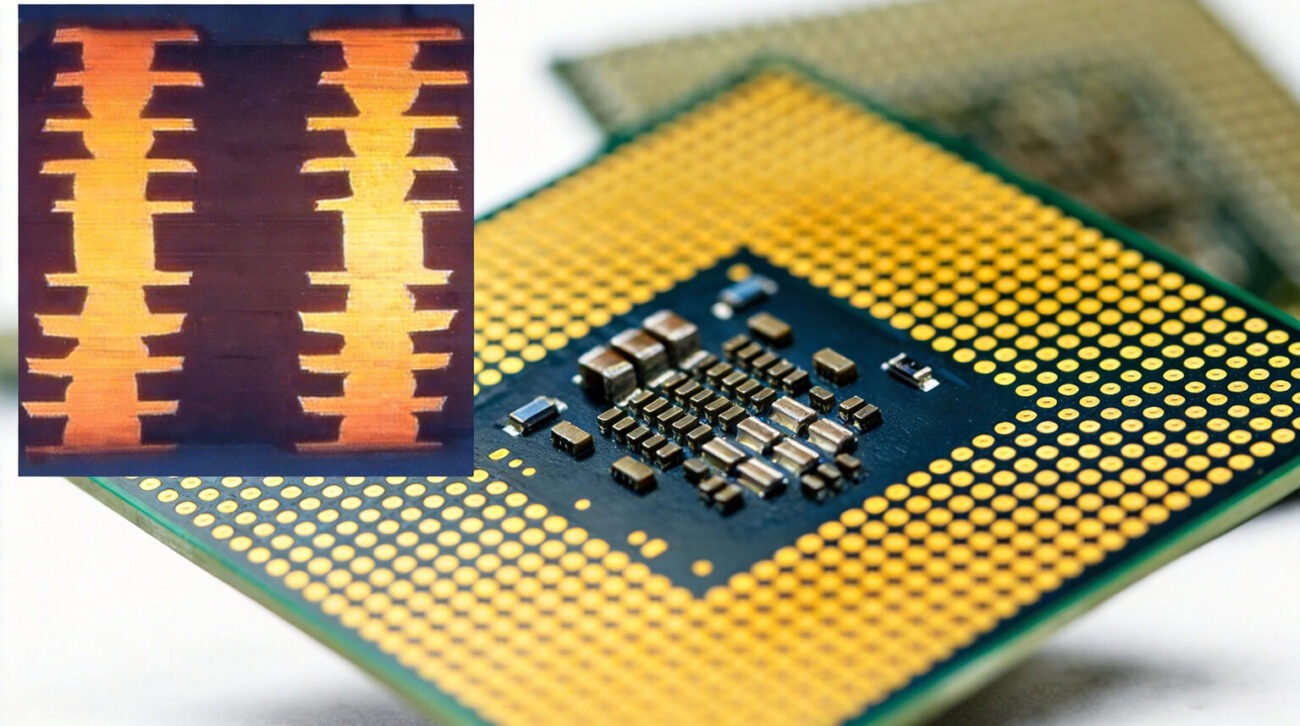
Any-Layer PCB Design Guide: From Concept to Manufacturing
Any-Layer PCB is a cutting-edge HDI technology that enables flexible routing for complex designs. This article provides a comprehensive guide from concept to manufacturable design.
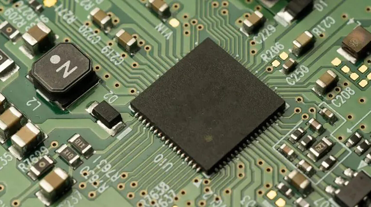
1+N+1 Stackup Design Tutorial for HDI PCB Board
Learn what 1+N+1 HDI PCBs really mean, including stackup structure, microvia and via types, sequential lamination, electrical advantages, and common design mistakes engineers should avoid.

2+N+2 Stackup Design Tutorial for HDI PCB Board
Learn how to design 2+N+2 stackups for HDI PCBs, including layer structure, microvia fanout, routing strategies, power distribution, and manufacturing considerations. A practical guide for engineers building high-density boards.
