When we talk about advanced electronics, the United States remains a market that cannot be ignored. Over the past few decades, many basic manufacturing processes have gradually shifted to Asia for reasons of cost and supply chain efficiency. However, in many high-tech products, U.S. companies still lead in R&D, system design, and core engineering definition.
The PCB industry follows the same pattern. In terms of global production volume, U.S. PCB manufacturing no longer holds a dominant position. Public information shows that the U.S. share of the global PCB market has dropped from more than 30% in 2000 to around 4% today. However, production volume does not fully represent industry value, and this becomes clearer when we look at specific market segments.
Take the aerospace and defense PCB market as an example. In 2025, the global market size was approximately USD 3.87 billion, with North America accounting for about 50.7%. A large part of this share comes from the U.S. market, which also shows that the U.S. PCB supply chain still has strong influence in high-compliance and high-reliability applications.
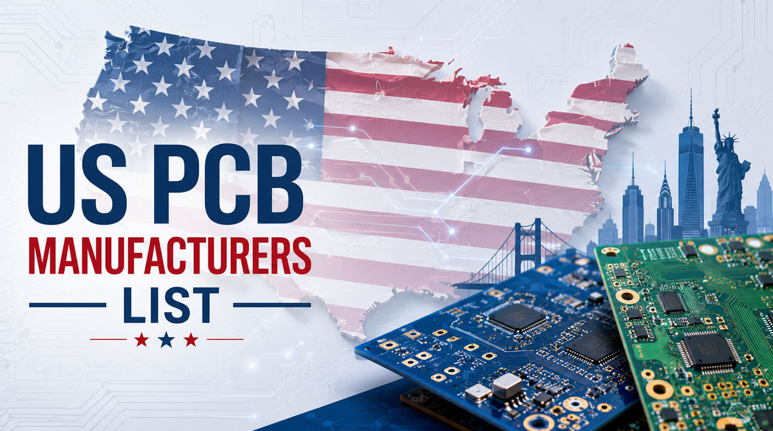
In this article, PCBCool looks at the market from the perspective of an industry competitor and lists 7 recommended American PCB manufacturers for 2026. The goal is to help engineers, procurement teams, and product companies find PCB manufacturing partners that are compliant, reliable, and truly suitable for their project needs.
Sierra Circuits is one of the more representative quick-turn PCB manufacturers in the United States. Founded in 1986, the company is headquartered in Sunnyvale, California. Its strength is not only PCB prototyping. Sierra Circuits combines quick-turn prototyping, domestic manufacturing, engineering review, and online ordering tools into a relatively complete manufacturing and engineering support system.
Unlike some platforms that rely on outsourcing or only provide standard board services, Sierra Circuits has its own PCB manufacturing and assembly facility in Silicon Valley, covering about 70,000 square feet. For customers looking for EMS services, this is important because keeping manufacturing and assembly within the same system helps control engineering review, production scheduling, and delivery timing.
Sierra Circuits is generally seen in the industry as a supplier focused more on high reliability and complex project support than on low-cost mass production. One example helps explain this: a circuit board manufactured by Sierra Circuits for a CubeSat project remained intact after a rocket explosion and was later displayed at the National Air and Space Museum in Washington, D.C.
Therefore, for customers who need to quickly validate a design, revise versions repeatedly, or communicate directly with a U.S.-based team, Sierra Circuits is a typical option to consider.
| Item | Capability |
|---|
| Layers | 1–30 layers |
| Materials | FR-4, Polyimide, Advanced / Exotic Materials, RF / Microwave Materials, Rogers, Teflon / PTFE, Hybrid Stack-ups |
| Board Thickness | .005″–.300″ |
| Copper Thickness | Up to 5 oz |
| Maximum Panel Size | 20″ × 30″ |
| Minimum Hole Size | Mechanical drill approx. .005″–.0059″; laser drill approx. .003″–.004″ |
| Minimum Trace / Space | 1.5 mil |
| Surface Finishes | Gold fingers, HASL, ENIG, OSP |
| Testing Capabilities | Electrical test, 100% net-list testing, TDR, microsection, solderability, X-ray fluorescence, ionic contamination, FAI, Certificate of Compliance |
| Quality Standards | IPC-6012 Class 1 / 2 / 3, IPC-6013 Class 1 / 2 / 3, Mil-spec / Class 3 / aerospace / medical |
| Certifications / Compliance | AS9100D, ISO 9001:2015, ISO 13485:2016, ITAR registration |
| Additional Services | DFM check, DFA check, BOM check, dedicated CAM engineer, online quotation, Turnkey PRO |
| Material Brands | Rogers, Isola, Nelco, Teflon / PTFE, Polyimide, and others |
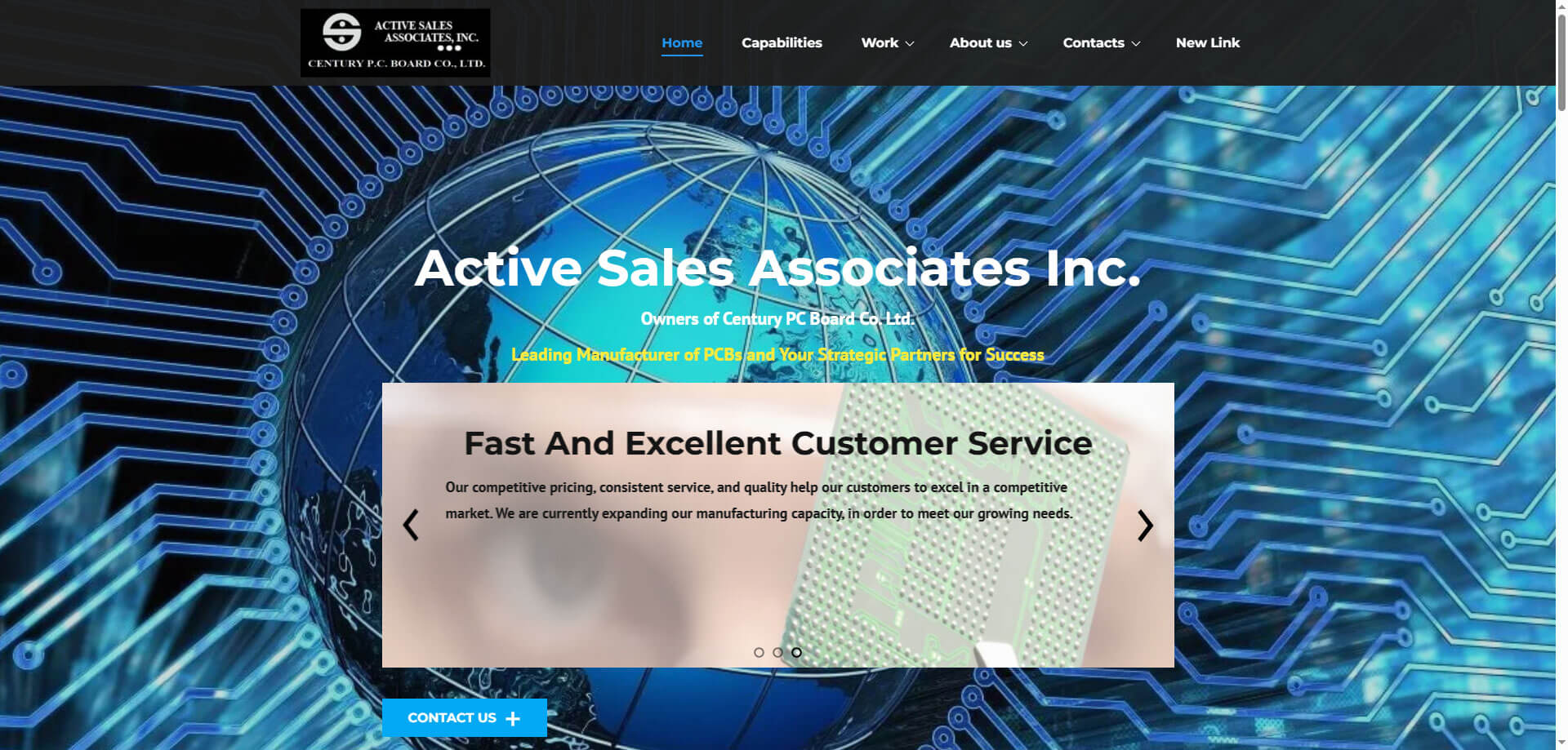
Active Sales Associates / Active PCB can be traced back to 1981, when it was founded by Alex Wu in Largo, Florida. Unlike some online PCB platforms that mainly focus on small-batch prototyping, Active PCB is positioned more toward prototypes, volume production, and long-term supply projects, mainly serving customers in North America.
The most noteworthy aspect is Active PCB’s business model: not a typical “U.S. office + U.S. local factory” model. Instead, it is closer to a “U.S. sales + Asian PCB manufacturing resources” supply system.
Based on public information, Active Sales Associates has a relationship with Century PC Board Co. Ltd., while Century PCB’s manufacturing resources are connected with PCB factories in Taiwan and Kunshan, China. Industry media Circuits Assembly has also described Active Sales Associates as the U.S. sales office for Century Taiwan and its sister company in China.
Therefore, Active PCB is better understood as a PCB sales, service, and supply chain window for the North American market, rather than simply a U.S.-based PCB factory or a basic trading middleman.
| Item | Capability |
|---|
| Layers | 2–36 layers |
| Materials | FR-4, RoHS Tg130–200, halogen-free materials, Rogers, Arlon, aluminum-based thermal materials, copper-based thermal materials |
| Board Thickness | 0.012″–0.200″ |
| Copper Thickness | Up to 5 oz |
| Minimum Hole Size | Laser via 0.004″; mechanical hole 0.006″ |
| Minimum Trace / Space | 0.003″ / 0.003″ |
| BGA Capability | 0.35 mm BGA pitch |
| Impedance Control | ±5% |
| Surface Finishes | HASL, lead-free HASL, ENIG, immersion silver, immersion tin, OSP, ENEPIG, hard gold, deep gold contact points |
| Certifications / Compliance | ISO 9001:2015 |
| Material Brands | ITEQ, Isola, TUC, Nanya, Rogers, Arlon, Ventec |
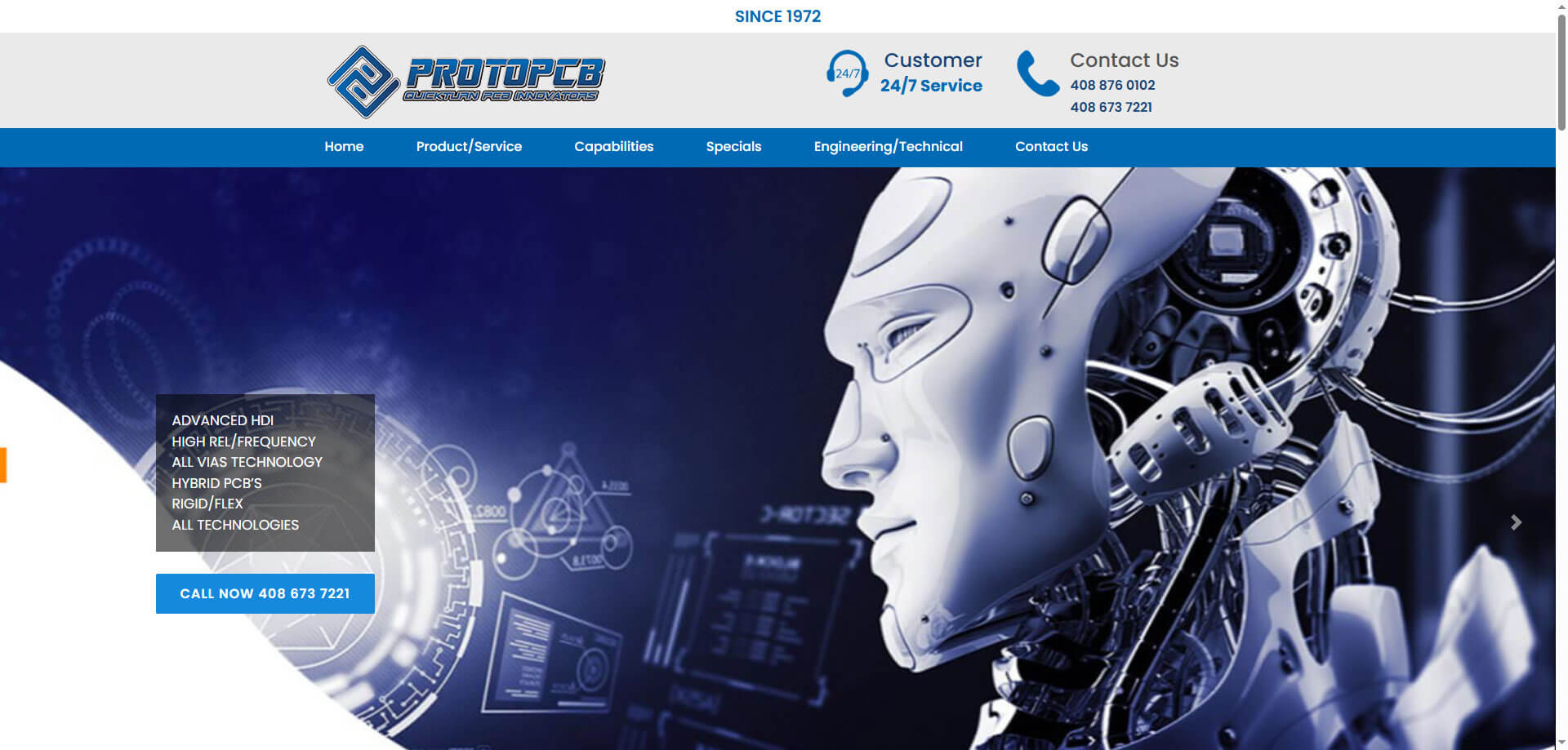
ProtoPCB was founded in 1972 and is headquartered in Milpitas, California. It is a PCB prototype manufacturer with a long history of serving the North American market. Compared with low-cost standard board platforms, ProtoPCB is positioned more toward engineering validation, R&D prototyping, and time-sensitive PCB projects.
According to public information, ProtoPCB has completed more than 1.1 million projects for the North American market and highlights an on-time delivery rate of 97.43%. The company can support 1–50 PCB pieces within 12–24 hours, and it can also support 1,000 pieces of 16-layer PCBs within 5 days.
From a manufacturing capability perspective, ProtoPCB has strong high-end bare board manufacturing capabilities. It can support multilayer boards up to 64 layers, heavy copper boards up to 10 oz, and 4+N+4 HDI structures. If a project involves relatively complex PCB prototyping, ProtoPCB is a supplier worth considering, although it may not be the cheapest option.
| Item | Capability |
|---|
| Layers | 1–64 layers |
| Board Thickness | Up to 10 mm |
| Copper Thickness | 10 oz |
| Minimum Hole Size | Laser hole 3 mil; mechanical hole 0.2 mm |
| Minimum Trace / Space | 1.5 / 1.5 mil |
| Engineering Support | DRC / DRM, 300+ checks, tolerance management, CAM engineer support |
| Quality Standards / Capabilities | IPC 610A Class 1 / 2 / 3 quality capabilities |
PS Electronics was founded in 2008 and is headquartered in Shenzhen, China. It is an electronics manufacturing service provider with a global manufacturing network, serving customers who need PCB manufacturing, PCB assembly, and complete product assembly support. The company operates PCB and PCBA manufacturing bases in China, works with PCBA manufacturing resources in Malaysia and Mexico, and also maintains a U.S. office to support international customers. To date, PS Electronics has completed more than 5,200 electronics manufacturing projects.
Unlike manufacturers that only provide bare PCB fabrication or standalone PCB assembly, PS Electronics focuses more on project-based manufacturing support. Each customer project is assigned a dedicated account manager, while the engineering team helps follow design review, production preparation, manufacturing progress, and delivery coordination. This makes PS Electronics more suitable for electronics projects that require continuous communication, cross-process coordination, and early identification of production risks.
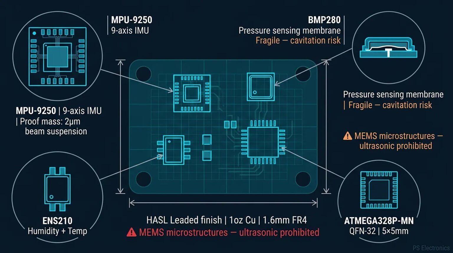
PCBCool is the digital online brand of PS Electronics. It is used for brand presentation, online consultation, project assignment, and quick quotation. For business customers, PCBCool can serve as an entry point to understand PS Electronics’ manufacturing capabilities and submit project requirements. For personal projects and student projects, it can also support quotation estimation and small-batch PCB order submission through the online ordering channel.
| Item | Capability |
|---|
| Layers | 1–40 layers |
| Materials | FR4 140Tg / 170Tg / 180Tg, halogen-free materials, metal-based materials, Rogers, Taconic, Teflon, hybrid stack-ups, and standard flexible material systems |
| Board Thickness | 0.3–6.5 mm |
| Copper Thickness | 1/3–33 oz |
| Maximum Production Size | 1500 × 600 mm |
| Minimum Board Size | 5 × 8 mm |
| Minimum Hole Size | Laser hole 0.08 mm; mechanical hole 0.15 mm |
| Minimum Trace / Space | 0.064 / 0.064 mm |
| Key Tolerances | Trace / space tolerance ±0.015 mm; hole size tolerance ±0.05 mm; board thickness tolerance ±5% |
| Surface Finishes | Lead-free HASL, ENIG, OSP, immersion silver, immersion tin, gold fingers, carbon ink, and others |
| Testing Capabilities | AOI, 100% electrical test, impedance testing, X-ray inspection, microsection analysis, solderability testing, dimensional inspection |
| Quality Standards | IPC Class 2 / 3, UL 94V-0 |
| Certifications / Compliance | ISO 9001:2015, ISO 13485:2016, ISO 14001:2015, REACH, RoHS, UL Canada |
| Production Capacity | 110,000 m² / month |
| Additional Services | DFM check, 24-hour expedited production, impedance control |
| Material Brands | KB, ITEQ, SY, ISOLA, Rogers, Ventec, Nelco, Panasonic, Taconic, and others |
Epec Engineered Technologies is a U.S. provider of custom electronic engineering and manufacturing solutions. Its history can be traced back to 1952, and the company is headquartered in New Bedford, Massachusetts. It is not a single PCB processing factory. Instead, it provides integrated manufacturing services for OEM customers around PCBs, custom electronic components, and engineering support.
One reason Epec deserves a place on a list of U.S. PCB manufacturers is its deep connection with the early development of the U.S. PCB industry. Its predecessors, Electralab and Printed Electronics Corp., were both connected with the early development of IPC. This gives Epec a certain historical significance in the U.S. PCB industry.
More importantly, Epec still maintains and integrates specific PCB manufacturing resources. Its NetVia Group has more than 35 years of experience and mainly serves time-sensitive engineering projects. UPE Inc. focuses on heavy copper and extreme heavy copper PCBs, and its PowerLink technology can support heavy copper printed circuit boards from 5 oz to 200 oz.
| Item | Capability |
|---|
| Layers | 1–40 layers |
| Materials | FR-4, high-speed / high-frequency materials, RF / microwave materials, flexible materials, rigid-flex materials |
| Board Thickness | 0.021″–0.125″ |
| Copper Thickness | Up to 200 oz |
| Maximum Production Size | 16″ × 22″ |
| Minimum Board Size | 0.5″ × 0.5″ |
| Minimum Trace / Space | 0.003″ |
| Surface Finishes | HASL, lead-free HASL, ENIG, immersion silver, OSP |
| Quality Standards | IPC Class 2 / 3 / 3A |
| Material Brands | DuPont, Panasonic, Rogers, Isola, Megtron |
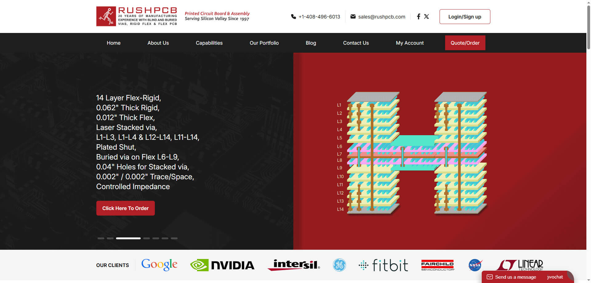
Rush PCB was founded in 1997 and is headquartered in Milpitas, California. It is one of the earlier PCB service providers in the U.S. market to offer online quotation and quick ordering access. This model allows it to serve not only business customers, but also hardware startups and electronics hobbyists with prototyping needs.
Rush PCB is not positioned only as a bare board manufacturer. For many engineering teams, a PCB project needs to solve the entire workflow from file submission to later assembly. Rush PCB provides services around this demand, covering each stage of turnkey electronics manufacturing.
It is also worth mentioning that PCB Trace is a publicly confirmable subsidiary of Rush PCB. It is used more to support Rush PCB’s market presentation in complex PCB areas such as high-layer-count boards, blind and buried vias, microvias, flexible boards, and rigid-flex boards. Therefore, when evaluating Rush PCB, PCB Trace can be viewed as part of its complex PCB capability presentation.
| Item | Capability |
|---|
| Layers | 1–40 layers |
| Materials | FR-4, special materials, high-speed / high-frequency materials, flexible materials, rigid-flex materials |
| Copper Thickness | 0.5–4 oz |
| Minimum Hole Size | 0.004″ |
| Minimum Trace / Space | 0.002″ / 0.002″ |
| BGA Capability | 0.35 mm BGA pitch |
| Quality Standards | J-STD-001, IPC-A-610E |
| Certifications / Compliance | ISO 9001:2015, ISO 13485:2016, ITAR, UL, RoHS, IPC |
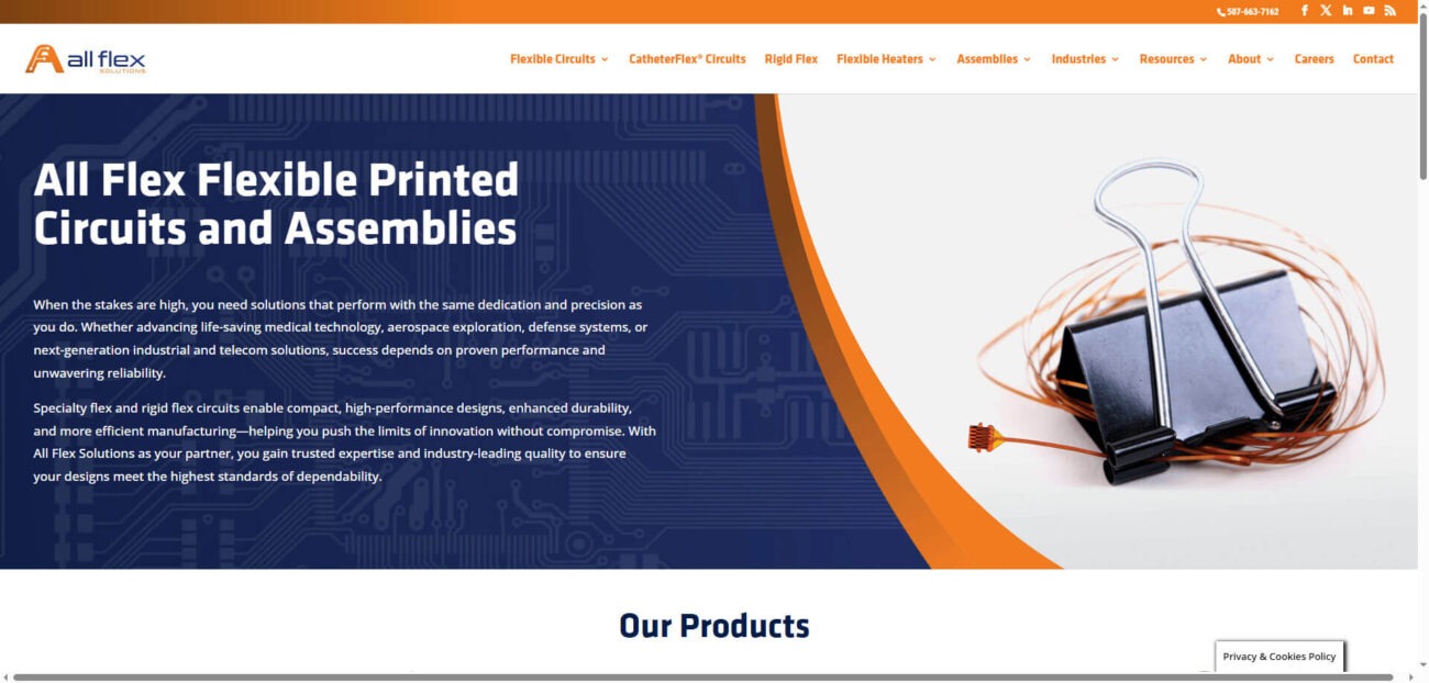
All Flex was founded in 1977 and is headquartered in Northfield, Minnesota. Unlike traditional general-purpose PCB factories, All Flex focuses on providing flexible circuit solutions. This relatively focused business model allows it to serve matching projects more effectively.
Medical applications are one of All Flex’s more representative fields. Its CatheterFlex® is designed for catheter-based medical devices. By using extended flexible circuits to reduce traditional wire connections, it improves space utilization and wiring stability in compact structures. This shows that All Flex is not only producing standard flexible PCBs, but can also provide more specialized flexible interconnect solutions around specific application scenarios.
In terms of quality systems, All Flex has AS9100, ISO 9001, MIL-PRF-31032, ITAR / JCP, RoHS, and IPC membership backgrounds. These qualifications match the requirements of high-reliability electronics projects.
For projects that require U.S.-based flexible PCB manufacturing, especially those with high requirements for space utilization, bending reliability, and structural stability, All Flex is a professional supplier worth attention.
| Item | Capability |
|---|
| Layers | 1–8 layers |
| Materials | Polyimide substrate, rolled annealed copper, electrodeposited copper, FR4 / PI stiffeners, metal reinforcement structures |
| Board Thickness | Minimum approx. 1 mil dielectric level |
| Maximum Board Size | Up to approx. 44 feet in length |
| Surface Finishes | ENIG, tin, silver, OSP, organic coatings |
| Testing Capabilities | In-circuit electrical testing, ionic contamination testing |
| Quality Standards | IPC 6013 Class III |
| Certifications / Compliance | AS9100D, ISO 9001:2015, ITAR, MIL-PRF-31032, UL, RoHS, JCP, ANSI/ESD S20.20 |
As one of the earliest regions to develop the printed circuit board industry, the United States has a relatively mature manufacturing system, with capabilities covering multiple specialized areas. Overall, however, the core advantage of the U.S. PCB supply chain is not cost. It is more reflected in engineering capability, compliance systems, and local manufacturing responsiveness.
In actual supplier selection, if a project is more cost-sensitive, some PCB manufacturers in Mexico can often offer a certain balance between delivery time and cost because of their geographic location and industrial structure. For this reason, they are also often used as a supplementary option within the North American supply chain system.
In general, whether choosing a PCB manufacturer in the USA or another region, the key is still the fit between supplier capability and project requirements. In the actual evaluation process, using a platform with supply chain information and engineering support capabilities can help reduce communication costs and improve supplier selection efficiency.

 Website: https://www.protoexpress.com/