PCB design tools today are increasingly built around collaboration, shared libraries, and cloud-connected workflows. CircuitMaker stands out in this space by combining professional-grade PCB design features with a community-driven platform where users can explore, learn from, and build on real projects created by others. That makes it more than just a design tool. It is also a practical environment for learning and improving your workflow.
In this tutorial, I will walk you through the complete process of designing and checking a simple two-layer PCB in CircuitMaker. The goal is to keep everything clear, practical, and easy to follow, whether you are new to PCB design or just getting started with this software. By the end, you will have a complete set of design files, a verification report, and a board layout that is ready for manufacturing. Let’s get started.
As mentioned earlier, CircuitMaker is cloud-connected, so your projects are stored online and can be accessed from anywhere. That makes the first step simple: create a new project in your workspace.
Here is how to do it:
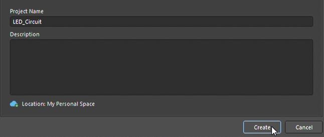
- Launch CircuitMaker and click Create a New Project on the home screen. This will open a dialog box.
- Next, enter a name for your project. Choose something clear and descriptive, such as LED Switch Board. You can also add a short description if needed.
- After that, select a folder in your online workspace. The default folder is usually fine if you do not need a custom location.
- Click Create to open the design interface. CircuitMaker will automatically generate a schematic file (.Sch) and a PCB file for the project. You will see both files listed in the Projects panel.
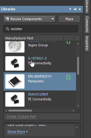
One of CircuitMaker’s biggest advantages is its large community-supported component library. Instead of working with generic placeholders, you can search for real manufacturer parts that are already linked to the essentials you need for design, including the schematic symbol, PCB footprint, and often a 3D model.
To place components, follow these steps:
- Open the Schematic tab, then click the Libraries panel on the right side of the screen.
- Use the search bar to look for the component you need. For example, you might search for ATmega328P if you are building an Arduino-style design, or RES if you want to add a resistor.
- As you search, CircuitMaker will display matching parts from different manufacturers and suppliers. Each entry typically includes the linked schematic symbol, PCB footprint, and 3D model information.
- Once you find the right part, click and drag it from the library panel onto the schematic sheet.
If you need more than one of the same part, simply drag it onto the sheet again. You can also rotate a component before placing it by pressing the Spacebar.
The schematic is the logical blueprint of your circuit. At this stage, you are not worrying about the physical placement of parts on the board. Instead, you are defining how everything is electrically connected. Those logical connections will later be translated into physical copper traces on the PCB, so a clean schematic is the foundation of a reliable design.
To start wiring the circuit, follow these steps:
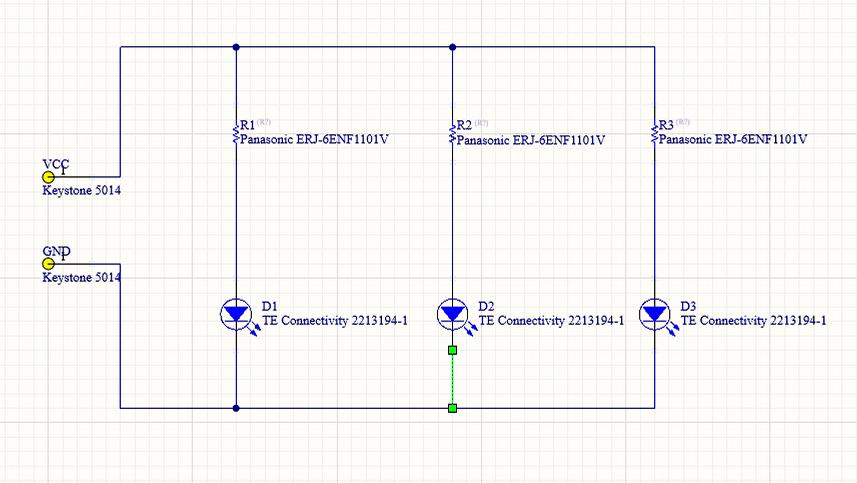
- Go to the top toolbar and select Place Wire, or simply press W on your keyboard.
- Click the pin where you want to begin the connection. CircuitMaker will highlight the connection point for you.
- Move the cursor to the pin you want to connect, then click again to complete the wire. CircuitMaker will automatically create a clean angled connection between the two points.
- Repeat this process until all required connections are in place.
For power and ground, use the Power Port tool from the top toolbar instead of drawing wires manually. This is the standard way to add connections such as VCC and GND, which you can select from the dropdown menu.
You can also use Net Labels to make the schematic cleaner and easier to read. To use a net label, click on a wire and assign it a name. Any other wire with the same label will automatically be treated as connected.
In CircuitMaker, when you choose a real, orderable part, the schematic symbol and PCB footprint are usually already linked for you. That means you do not have to assign footprints manually in most cases. Even so, it is still important to check that everything is correct before moving on.
Here is how to verify a component:
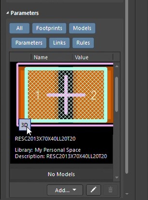
- Double-click any component in the schematic to open its properties.
- In the Properties window, go to the Models section. There, you will see the linked PCB footprint, such as 0805 or DIP-28. If available, you may also see an associated 3D model.
- Take a moment to confirm that the footprint matches the actual package of the part you intend to use.
Once the schematic is finished, the next step is to begin working on the actual board layout. This is where your circuit starts to take physical form. CircuitMaker keeps the schematic and PCB layout linked, so any design data transferred from the schematic to the board stays consistent. This workflow is commonly known as design synchronization.
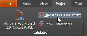
To update the PCB from the schematic, follow these steps:
- Go to the top menu and select Design > Update PCB. This will open a window called Engineering Change Order.
- In that window, CircuitMaker will list all the actions needed to bring the PCB in sync with the schematic. This can include adding new components, removing old ones, and updating net connections. Click Validate Changes to check the update. If everything looks correct, you should see green check marks.
- Next, click Execute Changes to apply the update.
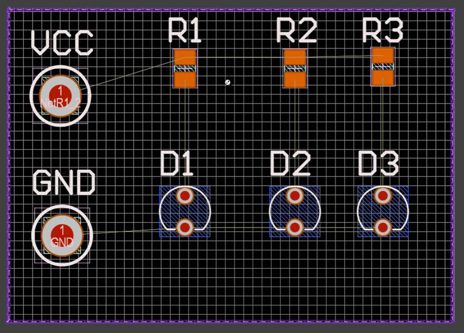
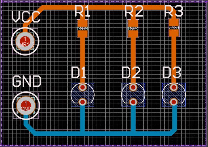
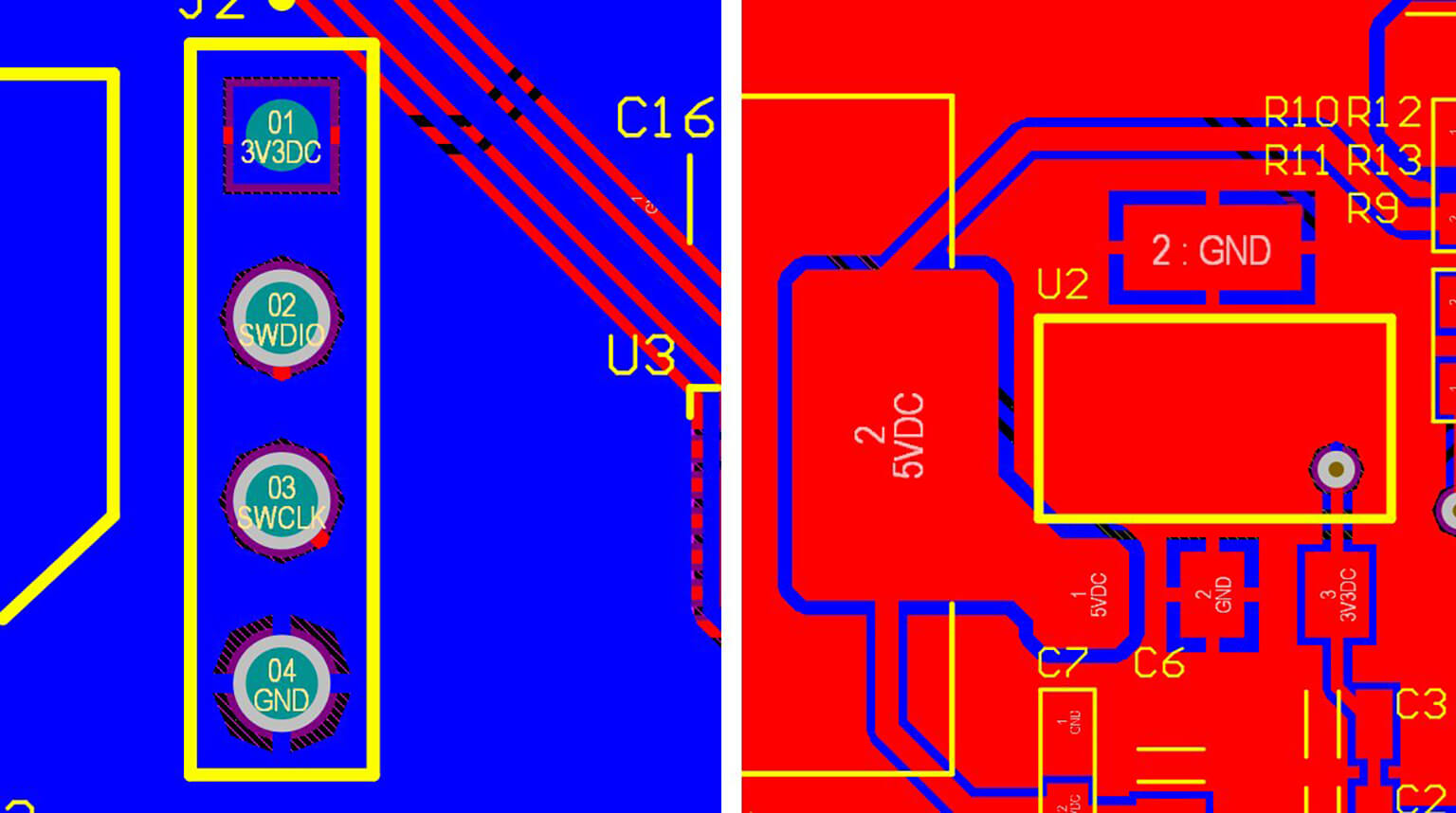
- After that, CircuitMaker will switch to the PCB document automatically. You will see all of your component footprints placed together inside an area called a Room, along with a set of thin blue airwires. These airwires show the electrical connections that still need to be routed on the board.
For a standard two-layer PCB, you will be working with two copper layers: one on the top side of the board and one on the bottom. As you move through the layout process, it is important to keep track of which layer you are using for routing, outlines, and markings.
At the bottom of the PCB editor, you will see the Layers panel. This is where you can view and switch between the different board layers. The main layers you will use are:
- Top Layer: The top copper layer, commonly used for routing and for placing surface-mount components.
- Bottom Layer: The bottom copper layer, also used for routing.
- Top Overlay: The silkscreen layer, where component outlines, reference designators, and other printed text appear.
- Mechanical 1: A mechanical layer often used for the board outline and dimension information.
As you work on different parts of the design, you will switch between these layers depending on what you are editing.
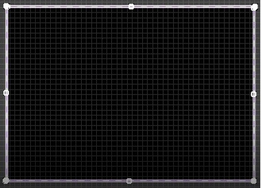
Before you can place components and route traces, you need to define the physical shape of the PCB. This outline represents the finished size and boundary of the board.
To create the board shape in CircuitMaker, follow these steps:
- Select the Keep-Out Layer and make sure it is visible.
- Then go to Design > Board Shape > Define Board Shape from the top menu. Once you enter this mode, the cursor will change and the rest of the workspace will appear dimmed.
- Click to place the corners of the board outline. If this is your first design, a simple rectangular shape is usually the easiest place to start.
- When you are done placing the corners, right-click to exit board shape mode. The area outside the board outline will remain dimmed, making the actual board boundary easier to see.
- Once the board shape is defined, you can begin dragging the component footprints from the Room onto the board for placement.
Good component placement is one of the most important parts of board design because it directly affects routing, performance, and manufacturability.
A well-planned layout helps you:
- Reduce routing complexity
- Improve electrical performance
- Make assembly easier
To place components more effectively, follow these steps:
- Use the Move command to drag components onto the board.
- Start with connectors, switches, and other parts that need to sit at the board edge or in a fixed physical position.
- Next, place the main components, such as microcontrollers or other ICs, in logical locations near the center of the board or wherever they make the most sense for the design. Then arrange their related supporting parts, such as resistors, capacitors, and crystals, nearby.
- Try to keep connected components close to each other. Shorter distances usually make routing easier and help reduce unnecessary trace crossings.
If you need to change a part’s orientation while placing it, click the component and press the Spacebar to rotate it.
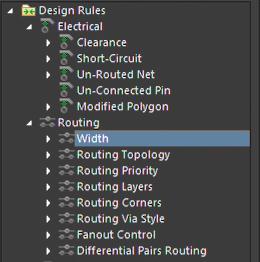
Design rules are one of the most important parts of PCB layout because they define the manufacturing limits your board has to follow. In other words, they set the minimum requirements for things like trace width, spacing, and other physical constraints. If these rules are too aggressive, the board may be difficult or expensive to manufacture. If they are set properly from the beginning, the layout process becomes much smoother.
To configure the basic design rules in CircuitMaker, follow these steps:
- Go to the top menu and select Design > Rules. This opens the PCB Rules and Constraints Editor.
- In the editor, expand Electrical and select Clearance. This is one of the most important settings for beginners.
- The clearance rule defines the minimum allowed distance between any two copper objects. A common safe starting value is 0.25 mm, although the exact number should match your manufacturer’s capabilities.
- Next, go to Routing > Width to set the allowed trace width.
- When you are done, click Apply and then OK. CircuitMaker will use these rules as you continue the layout, helping you avoid spacing and routing errors during the design process.
At this stage, you will turn the light blue connection lines, often called airwires, into actual copper traces on the board. CircuitMaker supports both manual routing and autorouting, but manual routing is usually the better choice when you are learning because it gives you more control over the layout.
To route the board manually, follow these steps:
- Go to the top toolbar and select Interactive Routing, or press P to use the Place Track command.
- Before you begin, make sure the correct trace width is selected, such as 0.25 mm, and confirm that you are routing on the intended layer, such as the Top Layer.
- Click on a component pad to start the trace, then move the cursor toward the destination pad. As you route, CircuitMaker will display helpful information such as trace length. It will also show a preview of the path and help guide the trace around nearby objects.
- If you need to switch layers while routing, press the * key on the numeric keypad. CircuitMaker will automatically place a via and continue the route on the other layer.
- When the trace reaches the target pad, click to complete the route.
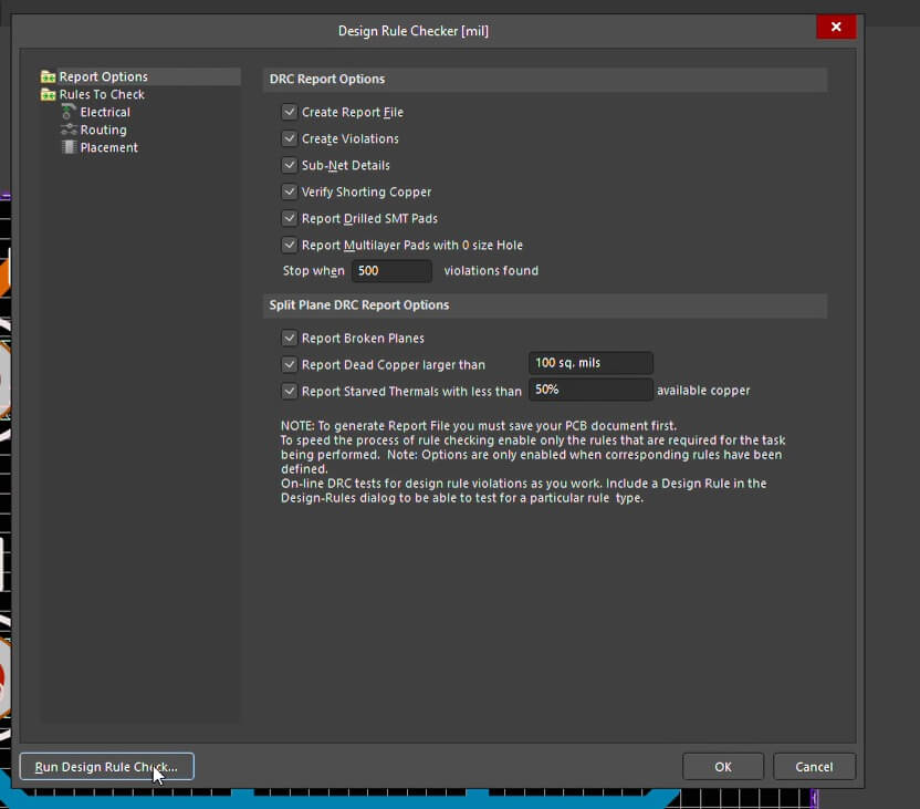
This is one step you should never skip. A design rule check, or DRC, is your final safeguard against common but costly mistakes such as shorts, missing connections, or clearance violations.
To verify the board, follow these steps:
- Go to Tools > Design Rule Check and start the DRC process.
- CircuitMaker will analyze the board against the rules you set earlier and generate a report showing whether any problems were found.
- If the report lists any violations, review them carefully and fix them before moving on.
- It is also a good idea to open the 3D Viewer and inspect the board in 3D. This gives you a more realistic view of the finished PCB and can help you spot placement or clearance issues that are easier to miss in the standard layout view.
By following these steps, you have completed the full PCB design workflow in CircuitMaker, from selecting real components to preparing the files needed for manufacturing. While this example focused on a simple two-layer board, the same basic process applies to many modern PCB designs.
If you are just getting started, begin with simple circuits and gradually work your way up to more complex designs as your confidence grows. With practice, you will be able to turn ideas into working hardware much more efficiently.
Once your design is ready for production, PCBCool can help bring it to life. We provide PCB manufacturing and assembly services for both companies and hobbyists, with support for everything from prototypes to production runs. Whether you are building your first board or managing a more advanced project, our team can help you move from design files to finished hardware with less hassle.