Power supply circuits are often designed first on paper, but they succeed or fail on the PCB. A regulator may meet its datasheet requirements and still create ripple, heat, or EMI problems if the board layout cannot support the way current actually moves.
On a real PCB, power delivery is physical. The distance between a capacitor and a switching device, the width of a high-current path, the return path under the load, and the heat path below a power component can all change how stable the circuit becomes during operation.
This article looks at PCB power supply design from that practical board-level perspective. Instead of treating the power supply as only a schematic block, it focuses on how to make the design work reliably after fabrication, assembly, and testing.
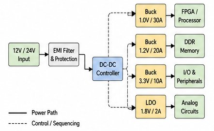
The power architecture of a multi-rail PCB is selected according to the load current, conversion efficiency, transient response, startup sequencing, and thermal limits of the system. A board with an FPGA, processor, DDR memory, analog blocks, and communication interfaces may need several rails supplied from one main bus.
For high-current, low-voltage FPGA and processor core loads at 1 V and 1.2 V, synchronous buck regulators are commonly used in the 500 kHz to 2 MHz frequency range. This helps reduce conduction loss while keeping the passive components compact enough for dense PCB layouts.
Power sequencing is also important. Processors and DDR memory devices often require controlled startup timing, monotonic voltage ramps, and tolerance limits of ±3%. If the rails are not sequenced correctly, latch-up conditions can occur and the device may power up in an unstable state.
In a distributed power architecture, power converters are placed close to high-current loads. This reduces copper loss because the IR drop across planes and vias becomes smaller. The tradeoff is that switching noise and thermal density are spread across more areas of the board.
In an intermediate bus architecture, the primary voltage source is usually 12 V or 24 V, followed by local step-down converters. This method reduces the length of high-current distribution and improves the efficiency of low-voltage power delivery.
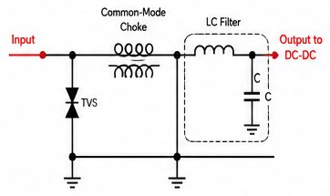
The input protection circuit protects downstream DC-DC converters from surge transients, reverse polarity, conducted energy, and inrush current stress. For 12 V DC-DC converters in industrial applications, TVS diodes are selected according to standoff voltage, clamping voltage, and peak pulse current rating based on IEC 61000-4-5 surge requirements.
For these 12 V converters, the TVS breakdown voltage should be between 13.3 V and 14.7 V. This prevents the TVS diode from conducting during normal operation while still allowing it to clamp abnormal surge events.
Input EMI filtering usually combines common-mode chokes, ferrite beads, and LC differential filters. The cutoff frequency should be well below the switching harmonics of the converter. At the same time, the filter must not create excessive impedance interaction with the DC-DC converter input stage. If the circuit is not damped properly, resonant peaks can appear and cause instability at the regulator input.
Layout is also part of the filtering strategy. High di/dt loops from the input capacitors, switching MOSFETs, and regulator path should be kept as small as possible. Low-ESR and low-ESL ceramic input capacitors should be placed within a few millimeters of the switching devices to reduce high-frequency current ripple and conducted EMI.
The regulator topology is selected according to the input voltage range, output current, efficiency target, noise tolerance, and thermal dissipation limit. Buck regulators are used when the input voltage is greater than the output voltage. With high-frequency switching converters, they can achieve efficiencies greater than 90%.
Boost regulators are used when the output voltage must be higher than the input voltage. They store energy through an inductor during switching and are often used in battery-powered systems where the input voltage can fall below the required rail voltage during discharge.
Switching frequency affects both size and loss. Higher switching frequency allows smaller inductors and capacitors, but it increases MOSFET switching loss and can increase radiated emissions. The inductor saturation current rating must exceed the peak inductor ripple current so that the regulator remains stable during dynamic load changes.
LDO regulators are commonly used for low-noise analog rails because they provide higher PSRR than switching converters. When selecting an LDO, the dropout voltage, load transient response, and output capacitor ESR must be verified.
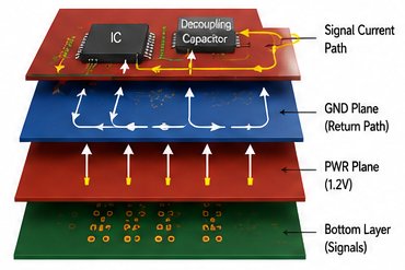
Power plane geometry directly affects IR drop, loop inductance, thermal spreading, and transient current delivery. Copper planes are preferred over narrow routed traces because they provide lower plane inductance at high frequency and a better transient response when the load switches.
The transition from a copper plane to a routed trace should avoid narrow neck-down regions. These areas can become localized current chokes, creating resistive loss and elevated temperature in high-current applications.
At high frequency, return current follows the path of lowest impedance rather than the path of lowest resistance. It tends to remain under the forward current path because of electromagnetic coupling between adjacent planes. If a plane split forces the return current to detour, the loop inductance increases and voltage noise can appear on the shared ground.
Via arrays are commonly used to reduce current crowding and interplane impedance. Multiple parallel vias should be used for high-current rails because the current capacity of a single via is limited by barrel resistance and copper thickness.
The dimensions of high-current conductors should be determined by the allowed temperature rise, current density, copper thickness, and surrounding thermal conditions. IPC-2152 provides guidelines for current-carrying capacity. For example, an external copper trace carrying 10 A may need to be several millimeters wide, depending on the allowed temperature rise and airflow.
Increasing copper thickness from 1 oz to 2 oz reduces conductor resistance and improves thermal spreading. This is especially important for power conversion paths that conduct more than 10 A.
Current crowding can occur at connector pins, vias, and narrow trace transitions. To reduce localized heating, the conductor geometry should be smooth, abrupt neck-downs should be avoided, and at least two parallel copper paths should be used where practical.
Power devices such as MOSFETs, voltage regulators, and power inductors often use thermal vias placed below the component body. These vias conduct heat into inner copper layers and help reduce junction temperature. Via diameter, pitch, and plating thickness all affect vertical thermal conductivity.
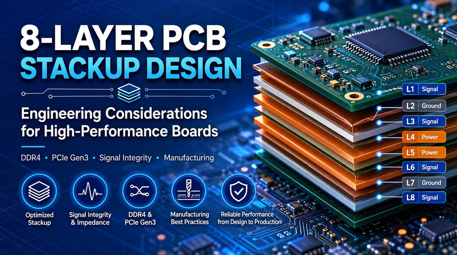
Balanced copper distribution in the multilayer stackup is also important. If copper distribution is uneven, the board can expand differently during reflow. This may cause PCB warpage and increase solder joint stress near high-current power devices.
The layout of a switching regulator directly affects output ripple, conducted EMI, transient stability, and switching efficiency. The high di/dt loop formed by the input capacitor, high-side MOSFET, low-side MOSFET, and switching node should be kept as small as possible.
This loop contains parasitic inductance. When the switching current is large, even a few nanohenries can create several volts of transient spike. The ESR and ESL of bypass capacitors also affect how switching current propagates across the PCB. For this reason, bypass capacitors should be placed close to the VIN and GND connections of the regulator.
The switch node should also be kept compact. Excessively large exposed copper at the switch node increases capacitive coupling to nearby nodes and increases radiated emissions.
Feedback traces should be routed away from the inductor and switch node so that ripple is not injected into the regulation loop. The analog feedback ground should remain separate from the high-current power ground until it connects at the controlled reference ground point of the regulator.
Power integrity validation confirms whether the PCB power distribution network can maintain stable voltage during dynamic loads and switching events. PDN impedance is often assessed with a vector network analyzer over a wide frequency range to confirm that it stays below the target value.
Excessive impedance peaks indicate anti-resonance. These peaks can occur when decoupling capacitors are not placed effectively or when the inductance of the power planes interacts with the capacitor network.
An oscilloscope is used to measure switching noise, voltage overshoot, voltage drop, and load step response. Measurement setup is critical. Long ground leads, insufficient probe bandwidth, or incorrect grounding can add artifacts that are not part of the actual switching behavior. Differential probes with adequate bandwidth and low inductance are preferred for accurate measurements.
Thermal validation is equally important for high-current power devices. Infrared thermal imaging and thermocouples can be used to find hot spots around MOSFETs, inductors, vias, and copper neck-down regions. Long-term reliability can be affected if junction temperature exceeds the derating limits specified for the component.
PCB power supply design becomes reliable only when the schematic, layout, and physical PCB structure are developed as one system. A regulator may be correctly selected, but the final board still needs to support stable current flow, clean switching behavior, and long-term operation under real working conditions.
For power-related products, this requirement becomes even more important. The PCB is not just a place to mount components; it directly affects how efficiently and reliably the product delivers power in the field.
PCBCool has practical experience with power supply boards, industrial power products, and energy-related electronics. If you are developing this type of project, our power & energy PCB solutions can help you move from design review to reliable PCB manufacturing and assembly.