0 M+

Monthly Capability

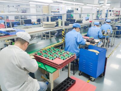
global manufacturing

0 +

Years of Experience

certified, traceable

< 0

Days for Delivery

prototyping in 3 days
0 +

Successful Projects

trusted by 450+ companies

01

Pre-Production

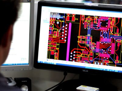
We begin every project with thorough preparation to ensure manufacturing success and minimize costly errors downstream.

02

SMT Assembly

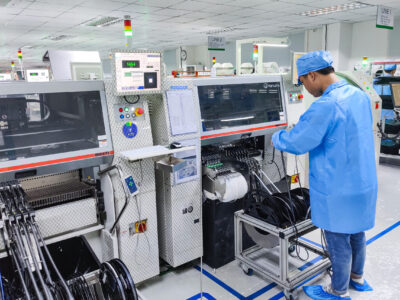
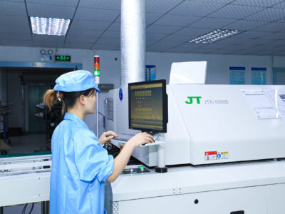
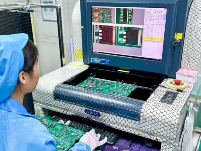
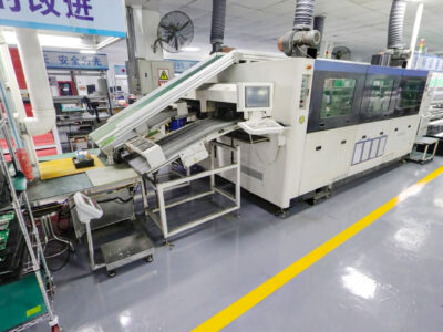
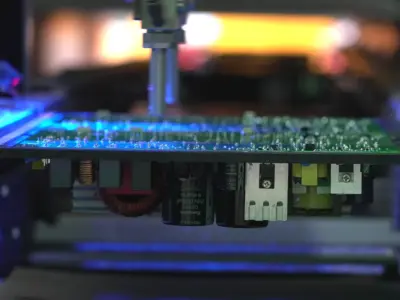
State-of-the-art surface mount technology with nitrogen reflow and multi-stage inspection for optimal solder joint quality.

03

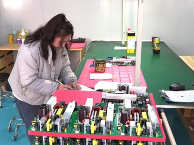
Through-Hole Assembly

Expert handling of through-hole components including large connectors and high pin-count devices.

04

Cleaning & Coating

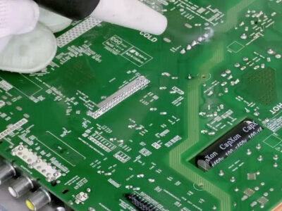
Protect your assemblies from environmental factors with our comprehensive cleaning and coating services.

05

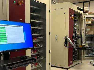
Testing & Quality Control

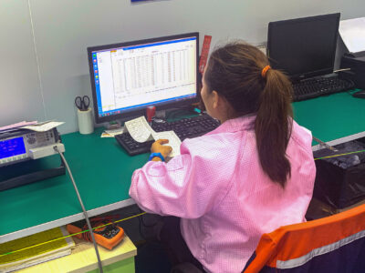
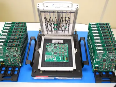
Rigorous multi-stage testing ensures every board meets specifications before shipment.

06

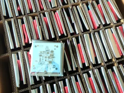
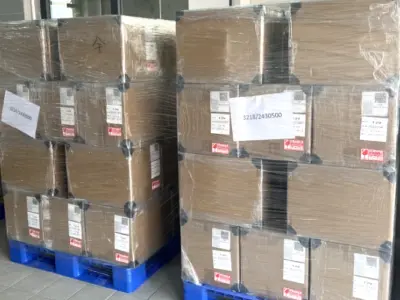
Packaging & Delivery

Secure packaging and efficient logistics ensure your products arrive safely and on time.

Global Facilities · Fast Delivery

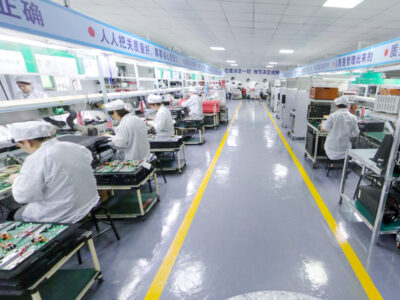
CoolPCB operates a global PCBA manufacturing network with facilities in Mexico, Malaysia, and China, complemented by branches in multiple regions. We offer clients fast delivery and a personalized, face-to-face experience.

Mexico circle

Mexico — Nearshore Speed for North America

  • 6 SMT production lines
  • Nearshore advantage for North America
  • Reduced logistics costs and tariffs
  • Lead time: 14-21 days for production
Malaysia circle

Malaysia — Cost‑Optimized & Stable Output

  • 9 SMT production lines
  • N₂ generator and nitrogen reflow capability
  • AI/MI assembly lines
  • Lead time: 7-28 days for production
China circle

China — Full Stack & High Capacity

  • 5 SMT production lines
  • Quick-turn prototype capability
  • Flexible small to mid-volume runs
  • Lead time: 3 days for prototypes, 7-21 days for batches

Quality Assurance & Traceability

At PCBCool, every PCB Assembly project is backed by globally recognized certifications and a strict quality management system to ensure safety, reliability, and compliance in every build.

Factory certifications

Factory Certifications

  • ISO9001 — Quality Management Systems
  • ISO13485 — Medical Device Quality
  • ISO14001 — Environmental Management
Product compliance

Product Compliance

  • UL — Safety Certification
  • RoHS — Restriction of Hazardous Substances
  • REACH — Chemical Safety and Environmental Compliance
1 high quality

Our Quality Commitment

  • Board-level barcode tracking records
  • Process data kept over 3 years
  • MES/ERP integration shows real-time quality metrics

FAQ

Q1: What file formats do you accept for PCB assembly quotes?

We accept Gerber files (RS-274X), BOM in Excel/CSV format, and centroid/pick-and-place files (XY coordinates). ODB++ and IPC-2581 formats are also supported. Our engineering team will review your files within 24 hours and provide DFM feedback.

Q2: What is your minimum order quantity for PCB assembly?

We have no strict MOQ for prototypes and accept orders as small as 5-10 pieces. For production runs, we recommend quantities of 50+ units for optimal pricing, though smaller batches are accommodated based on project requirements.

Q3: Do you provide Design for Manufacturing (DFM) services?

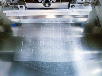
Yes, complimentary DFM/DFA analysis is included with every quote. Our engineers check for component spacing, pad geometry, stencil aperture design, thermal relief adequacy, and assembly clearances. We provide detailed reports with recommendations to improve manufacturability and reduce costs.

Q4: What components sizes can you assemble?

We handle components from 01005 (0.4mm x 0.2mm) chip components up to large connectors and transformers. BGA packages down to 0.25mm pitch are standard. We also support press-fit connectors, through-hole components, and mixed-technology assemblies.

Q5: How do you ensure quality for BGA and QFN packages?

All BGA, QFN, and other leadless packages undergo mandatory X-ray inspection to verify solder joint quality, check for voids, and detect bridging. Our X-ray systems provide real-time imaging with automated defect recognition algorithms.

Q6: Can you source components, or do I need to provide them?

We operate as a turnkey manufacturer and source all components through authorized distributors including Microchip, TI, Arrow, Avnet, Future Electronics, Element14, and Digi-Key. This ensures authentic parts with full traceability and eliminates counterfeit risk.

Q7: What testing options are available?

We offer flying probe testing, in-circuit testing (ICT), functional circuit testing (FCT) with custom fixtures, burn-in testing (24-72 hours), boundary scan testing, and environmental stress screening. FCT programs can be developed based on your functional specifications.

Q8: Do you support nitrogen reflow soldering?

Yes, our Malaysia facility is equipped with N₂ generators and nitrogen atmosphere reflow ovens. Nitrogen reflow reduces oxidation, improves solder wetting, and enhances joint reliability particularly for lead-free alloys and sensitive components.

Q9: How do you handle counterfeit component prevention?

We exclusively source from authorized distributors and franchised channels. All incoming components undergo date code verification, visual inspection, and sample testing. Our barcode warehouse system maintains complete chain-of-custody documentation from procurement through assembly.

Q10: What documentation do you provide with assembled boards?

Standard documentation includes First Article Inspection (FAI) reports, Certificate of Conformance (CoC), test data for ICT/FCT, X-ray images for critical components, and traceability reports. Additional documentation such as 8D reports and SCAR (Supplier Corrective Action Request) forms are available upon request.