If you’ve ever wondered why some PCB traces are drawn in serpentine or accordion-like patterns, this article is for you.
In an ideal world, electrical signals would travel from transmitter to receiver instantaneously. In reality, nothing moves faster than the speed of light—and on a PCB, signals travel significantly slower due to the materials involved. PCB traces behave as transmission lines, where electromagnetic waves propagate at a finite velocity determined by the dielectric environment.
This finite velocity introduces propagation delay: the time required for a signal edge (the rising or falling transition) to travel from one end of a trace to the other.
Propagation Delay in Real PCBs:
On standard FR-4 material—the most common PCB substrate, with a dielectric constant of approximately 4.0–4.5—signal propagation delay is well understood:
Typical propagation delay ranges from 140 to 180 picoseconds per inch (ps/in), depending on trace geometry and stackup.
- Microstrip traces (outer layers) usually fall around 140–150 ps/in.
- Stripline traces (inner layers) are slower, typically 160–180 ps/in.
In practical terms, this corresponds to a signal speed of roughly 6 inches per nanosecond, or about half the speed of light in a vacuum.
Not all signals require length matching. It should be applied only where timing skew can cause functional failures. In practice, this means focusing on high-speed interfaces where multiple signals must arrive within a tight timing window—often on the order of picoseconds. For all other signals, keeping traces short, direct, and clean is usually the better design choice.
LVDS signals are high-speed differential serial links, and the primary requirement is intra-pair length matching to minimize skew between the positive and negative traces. When multiple LVDS lanes are used in parallel (such as in some display or camera interfaces), maintaining lane-to-lane symmetry is also important.
For USB SuperSpeed interfaces:
- TX and RX differential pairs must be tightly matched within each pair, typically within 10–20 mils.
- There is generally no strict inter-pair matching requirement, but excessive skew should be avoided.
- USB4 operates at very high data rates and therefore has a much tighter timing budget, requiring careful control of both length and impedance.
These high-speed serial interfaces primarily require intra-pair length matching to preserve signal integrity. Lane-to-lane matching is typically handled at the protocol level and is far less critical than matching the positive and negative traces within each differential pair.
MIPI D-PHY interfaces impose strict limits on skew:
- Intra-pair matching is typically required to be within ~20 mils, depending on the SoC (e.g., NXP i.MX8).
- Clock-to-data and inter-lane skew is usually allowed within 100–500 ps, depending on lane count and operating mode.
- Multi-lane configurations (2 or 4 lanes) increasingly resemble bus-style matching, similar to DDR layouts.
Length matching refers to ensuring that all traces within a related group—such as a DDR data bus or a differential pair—have the same physical length, typically measured in mils or millimeters. This is usually achieved by adding tuning patterns (serpentine, accordion, or trombone routing) to shorter traces until they match the longest one.
Delay matching, on the other hand, focuses on ensuring that signals experience the same propagation delay, measured in picoseconds, regardless of their physical length. In practice, signal delay is determined by:
Physical length × propagation delay per unit length
In many PCB designs, length matching is a good approximation of delay matching—but only under specific conditions.
Length matching and delay matching are effectively equivalent when:
- All traces are routed on the same layer type (microstrip vs. stripline).
- Trace width and spacing are consistent.
- A solid, continuous reference plane is present (no splits or voids).
- The stack-up is uniform across the entire routing path.
When these conditions are not met, two traces with the same physical length can still experience significantly different delays, making delay matching the more accurate design goal—especially at very high data rates.
Differential signaling—used in interfaces such as USB, PCIe, HDMI, LVDS, MIPI, and Ethernet—offers excellent noise immunity and supports very high data rates. However, these benefits are only realized when the two traces within each differential pair (P and N) are well balanced.
There are two distinct types of length matching involved in differential routing:
- Intra-pair matching: matching the lengths within a single differential pair (P vs. N).
- Inter-pair matching: matching lengths between multiple differential pairs in a multi-lane interface.
Differential receivers operate by subtracting the two input signals:
Vdiff = VP − VN
When the two traces are equal in length, the P and N signals arrive at the receiver at the same time. This results in maximum common-mode noise rejection and a clean differential waveform.
If one trace is longer than the other, intra-pair skew is introduced. In this case, one polarity arrives later than the other, causing part of the differential signal to convert into common-mode noise. The consequences can include:
- Reduced noise margin
- Increased jitter
- Eye diagram closure
- Higher EMI emissions
- Increased bit error rate
For high-speed differential interfaces, tight intra-pair length matching is therefore critical to signal integrity.
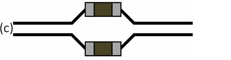
Serpentine and meander routing are commonly used techniques for adding trace length during length matching. While the two terms are often used interchangeably, several distinct routing styles exist—each with different signal integrity trade-offs.
Common Styles of Meander Routing:
This style uses tight, repeating U-shaped or semicircular bends placed perpendicular to the main trace direction—often described as a “snake-like” pattern. While widely used, overly tight spacing between segments can increase self-coupling and crosstalk, potentially reducing the effectiveness of length tuning.
This approach relies on longer U-turns routed parallel to the main trace direction, similar to extending a trombone slide. It is often preferred in dense layouts because it allows better spacing between segments, resulting in lower coupling and more predictable impedance behavior.
These patterns use angled (typically 45-degree) bends instead of sharp turns. While not strictly required, angled routing can help smooth impedance transitions and is sometimes chosen to reduce abrupt geometric changes along the trace.
A widely accepted rule of thumb for placing length tuning—such as serpentines, trombones, or accordion patterns—is to add the extra length as close as possible to the source of the mismatch (skew). In most cases, this means placing the tuning near the driver or transmitter, rather than at the receiver.
The reasoning is straightforward: length mismatches often originate at the fan-out region of the driver pins, where geometry constraints force traces to diverge unevenly. Correcting the mismatch close to its source minimizes the accumulation of additional skew and keeps the remainder of the routing path as uniform as possible.
A classic example is a differential pair that becomes mismatched during fan-out from the transmitter pins. Applying length tuning immediately after the fan-out restores symmetry early and preserves signal integrity along the rest of the route.
Vias are not just simple holes in a PCB—they introduce parasitic inductance and capacitance that can alter signal propagation. In high-speed designs, these parasitics can lead to timing skew, impedance discontinuities, and signal integrity degradation, all of which undermine effective length matching.
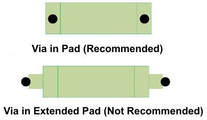
Placing vias directly in component pads (via-in-pad) can introduce additional inductance and capacitance, affecting the local impedance. If via pads remain on unused layers, the extra copper increases parasitic capacitance, which can result in an impedance drop.
When multiple vias are required, they should be staggered rather than aligned vertically or horizontally. Aligned vias can disrupt the return current path, forcing currents to detour around via antipads and reference plane voids. This increases loop inductance and can introduce unexpected skew and noise.
Via stubs are a common source of signal degradation in high-speed designs. Unused portions of a via act as resonant stubs, causing reflections and limiting effective signal bandwidth. To mitigate this:
- Minimize unnecessary layer transitions
- Keep stub lengths as short as possible
- Use back drilling when vias cannot be avoided
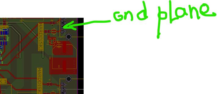
In high-speed PCB design, differential pairs rely heavily on a consistent reference plane—typically a solid ground plane—to maintain controlled impedance, tight coupling, low noise, and overall signal integrity. The reference plane defines the electromagnetic field structure of the pair and provides a low-impedance return path for any residual common-mode currents.
When a differential pair is routed over a continuous, unbroken reference plane, its impedance remains stable and predictable. In contrast, routing over a split or discontinuous plane forces return currents to detour around plane gaps, increasing loop inductance and introducing impedance discontinuities, skew, and additional noise.
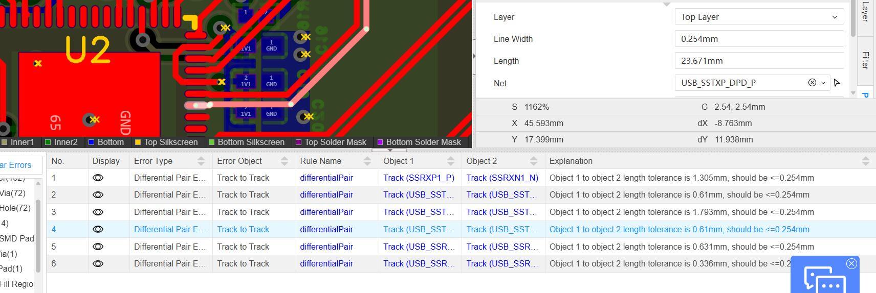
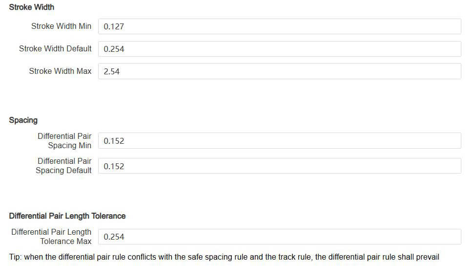
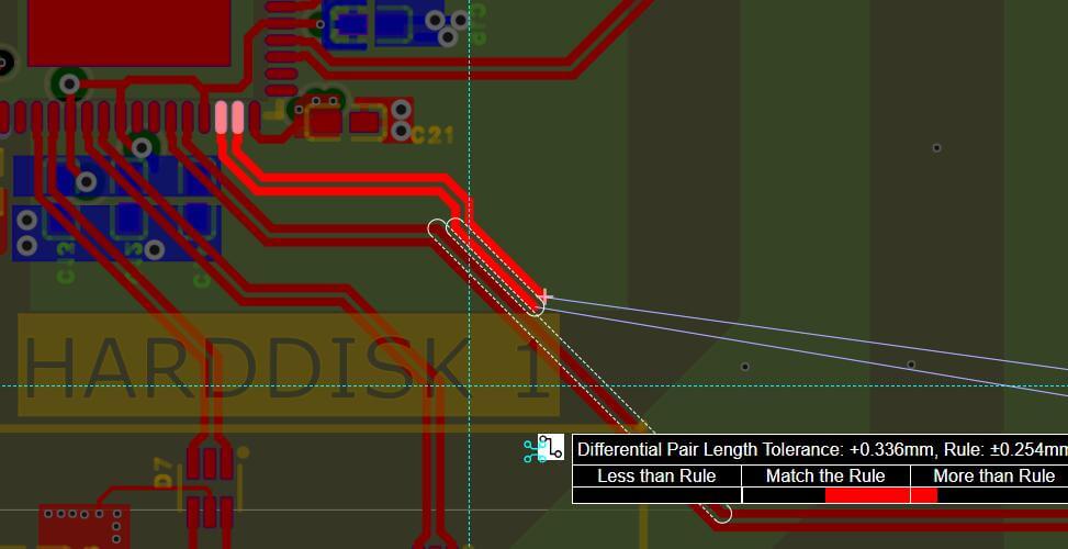
In high-speed PCB design, length matching tolerances define how precisely trace lengths must be equalized to avoid timing skew—the difference in signal arrival times that can lead to bit errors, reduced eye openings, or even link failure. These tolerances are typically defined by the interface specification or design guidelines (for example, JEDEC for DDR or PCI-SIG for PCIe).
In most PCB layout tools, length matching constraints can be set in the differential pair or routing rules. This allows the software to continuously monitor the routing and alert the designer when the length tolerance is exceeded.
For example, EasyEDA provides differential pair settings where you can specify maximum skew and other matching constraints.
During routing, these constraints can be used to verify whether the current trace lengths meet the required tolerance and to prompt corrective action if needed.
Length matching is a critical tool, but it is not the only requirement for reliable high-speed design. The goal is to match lengths where needed, keep routing clean and symmetric, respect vias and reference planes, and always treat signal integrity and EMI as co-equal constraints.
When these principles are followed, high-speed boards are more likely to meet timing requirements, maintain healthy eye diagrams, and pass EMC tests without surprises.
Length matching is a critical technique in high-speed PCB design for equalizing signal propagation delays and preventing timing skew, which can cause data errors in interfaces such as DDR5, PCIe, and high-speed SerDes. Using controlled serpentine or trombone meanders, designers can compensate for natural length differences caused by pin escapes, vias, or routing constraints.
Success depends on placing these tuning patterns close to the source of skew, maintaining consistent reference planes, and minimizing via asymmetries to preserve signal integrity. Tolerances are extremely tight and vary by interface—modern standards can require intra-pair matching on the order of ±2–5 mils, so following protocol specifications is essential.
Poorly implemented tuning can increase EMI, crosstalk, and impedance discontinuities, which is why wide spacing, smooth bends, and minimal added length are important. Ultimately, effective length matching balances precise timing control with robust signal integrity and EMC performance, making it a cornerstone of reliable high-speed digital systems.
If you need help turning your design into a manufacturable PCB, PCBCool offers high-speed PCB fabrication and assembly services with experience in DDR, PCIe, USB, HDMI, and other high-speed interfaces. Our engineering team can support length matching, impedance control, and signal integrity checks to help ensure your board meets performance and compliance requirements.