5G technology is reshaping modern wireless communication by enabling higher data rates, lower latency, and more reliable connectivity. As 5G systems continue to move into more demanding commercial and industrial applications, the performance of the PCB becomes increasingly important.
Unlike conventional circuit boards, 5G PCB must remain stable under high-frequency RF and mmWave conditions. At these frequencies, the PCB itself becomes part of the signal path, and small changes in material properties, routing geometry, via structures, or stack-up design can lead to measurable signal loss, impedance deviation, phase error, or reliability risks.
In this article, we will explain how these design constraints affect 5G PCB performance and discuss practical techniques that can be used to reduce signal loss, improve EMI containment, and enhance reliability in high-frequency PCB designs.
Understanding the dielectric characteristics of PCB materials is essential for material selection, process planning, and RF performance control, especially above 10 GHz. With the development of mmWave systems operating at 28 GHz and 39 GHz, variations in dielectric constant (Dk) can produce phase shift, change impedance, and cause inaccuracies in beam-forming systems used in phased-array architectures if the ΔDk exceeds 0.05.
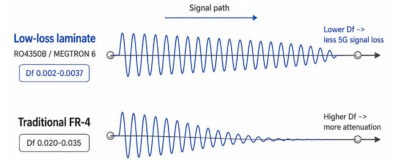
For example, low-loss laminate materials such as Rogers RO4350B have a Dk of 3.48 and a Df of 0.0037 at 10 GHz, while MEGTRON 6 has a Df of 0.002. In comparison, traditional FR-4 materials generally have Dk values between 4.2 and 4.5, with Df typically between 0.020 and 0.035, creating excessive losses through the RF signal transmission path.
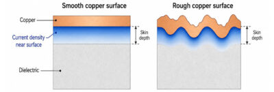
In addition to dielectric loss, conductor surface roughness becomes more dominant at higher frequencies. As frequency increases, skin depth decreases, making skin-depth-related loss more significant. For instance, the skin depth at 28 GHz for copper is 0.39 microns. Therefore, most of the current is concentrated near the surface of the conductor. As a result, a rough copper surface produces greater effective resistance and higher insertion loss than a smooth copper surface. This increased resistance and insertion loss is generally estimated by applying either Huray or Hammerstad correction factors as part of the EM simulation process.
To accurately obtain dielectric properties, designers can perform frequency-sweep measurements using split-post dielectric resonators, VNA-based insertion loss measurements, and S-parameter correlation between CAD simulation and physical measurement. These results can then be compared with 3D electromagnetic field modeling programs, including HFSS and CST Microwave Studio.
For 5G PCB transmission line design, deviations from the target impedance should not exceed 5% in order to achieve accurate electromagnetic modeling. Deviations greater than ±5% will greatly increase return loss and deterministic jitter on high-speed interfaces operating above 25 Gbps.
Fabricating a 50 Ω microstrip on an FR-4 laminate with εr of 3.48 and a dielectric thickness of 0.1 mm can result in trace widths ranging between 180 µm and 210 µm. This variance in trace width is due to copper thickness and etching compensation. Increasing conductor profile and dielectric variation can affect the effective impedance at frequencies higher than 10 GHz. Therefore, 2D field solver extractions alone may not provide sufficient accuracy for routing at mmWave frequencies.
The best practice for routing differential pairs in 100-ohm channels is to maintain a phase skew of greater than 1.5 ps to minimize mode conversion and eye closures. This is especially important because of the glass weave effect in PCB materials.
In general, RF channels operating at 28 GHz are routed using grounded coplanar waveguide structures rather than traditional microstrip routes. This is usually done because grounded coplanar waveguides provide a higher level of field confinement and lower radiation loss.
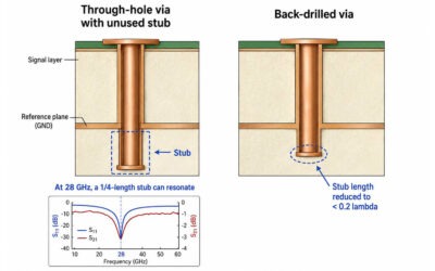
When designing high-frequency 5G PCB, via discontinuities introduce parasitic inductance of 0.6 to 1.2 nH for each mm of via barrel length. This can impact the S-parameters of the PCB at frequencies above 10 GHz. In a traditional through-hole via, the unused via barrel can behave as a quarter-wave stub when its electrical length reaches 1/4 of the operating frequency.
Therefore, at 28 GHz, the electrical length of a 1/4-length stub corresponds to 2.7 mm of the FR-4 equivalent effective dielectric. This behavior can create a sharp dip in impedance on S11 and cause degradation in S21 insertion loss.
Using back drilling will reduce the amount of unused vertical via barrel length to < 0.2 λ, thereby minimizing stub length and its associated resonant effects.
High-frequency return-loss performance can also be improved by reducing parasitic capacitance through proper anti-pad design. Increasing the anti-pad diameter from 1.5 times the hole size, combined with proper via field planning and via fencing at λ/20 spacing, helps maintain return-current continuity and suppress cavity resonance on reference planes.
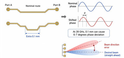
At mmWave frequencies, PCB layouts begin transitioning from lumped-circuit assumptions to distributed electromagnetic behavior. As a result, changes on the order of 0.1 mm can cause significant phase errors. For example, at 28 GHz, using a PCB material with ε_eff ≈ 3, the wavelength measured along the copper traces is about 6 mm, resulting in high sensitivity to interconnect length tolerances. A change in trace length of 0.1 mm will yield a phase deviation of 6 to 7 degrees, causing errors in the accuracy of phased-array systems for controlling beam direction.
Controlled coplanar waveguides are the preferred transmission medium due to superior electric field control. However, care must be taken to maintain ground-plane centerline symmetry and ±5 µm copper balance between reference points to prevent mode-field asymmetry and unintended radiation leakage.
Optimized tapered geometries are required to decrease return loss at transition points between RF IC pads and transmission lines. In many cases, 3- to 5-stage impedance transitions are used to provide smoother RF launches.
Antenna feed networks operating at 39 GHz and 77 GHz require highly isolated RF channels. When the distance between two adjacent channels is ≤ λ/20, such as 0.4 mm at 39 GHz, measurable mutual coupling can occur, with an isolation level greater than -20 dB. Surface-positioned ground stitching vias spaced at λ/10 or less can help suppress surface wave propagation while stabilizing return-current paths.
Copper surface irregularities can produce additional loss on the order of 15% to 25%. Therefore, very smooth copper surfaces and rolled foil are often selected to further minimize transmission loss in mmWave 5G PCB designs.
FPGA and 5G RF transceiver systems can experience fast voltage and current transients. To keep voltage ripple below 3% during instantaneous transient events with timescales below one nanosecond, the PCB must use a low-impedance power distribution network (PDN) capable of maintaining stable power delivery across the operating frequency range.
To determine the target impedance of the PDN, use the formula:
Z = ∆V / ∆I
For example, if the nominal FPGA supply voltage is 0.9 V, the allowable voltage ripple is 27 mV, and the transient current level is 12 A, the target PDN impedance should be less than or equal to 2.25 mΩ. This level of PDN impedance can be achieved using multiple parallel capacitor networks arranged so that the self-resonance frequencies of each network are not coincident with the frequency of operation for the FPGA and span across a bandwidth from kilohertz to several hundred megahertz.
Damping capacitors for this type of circuit must be selected with controlled equivalent series resistance (ESR) values between 20 and 80 mΩ. To further reduce current return inductance, the distance between the bottom power plane and the top ground plane should be kept to 50–75 µm.
For dense PCB designed for 5G applications operating above 10 GHz, electromagnetic coupling can occur between edge-coupled transmission lines due to fringing electric fields, discontinuous return paths, and common-mode current generation. When the centerline separation between adjacent transmission lines (TMLs) is less than or equal to three times the dielectric height (3H), coupling becomes more difficult to control.
If two edge-coupled TMLs are fabricated with centerline spacing less than or equal to 3H, the near-end crosstalk between the two TMLs can exceed -25 dB at 28 GHz. This can affect signal integrity, increase radiation risk, and reduce the noise margin of high-frequency 5G channels.
The effectiveness of the enclosure in which components are located depends on how well it is grounded. At 39 GHz, a 1 nH ground reference can create a reactive impedance of 245 Ω, which significantly reduces the overall performance and effectiveness of the shield by creating a high-impedance path.
Therefore, it is important to ensure that multiple low-inductance chassis bonds are used to contain incoming and outgoing EMI. Controlled chassis ground termination, perimeter via stitching, and proper return-path planning can help improve EMI containment and shielding performance in dense 5G PCB assemblies.
High-density 5G multilayer printed circuit boards experience significant thermo-mechanical stresses. These stresses arise from elevated radio frequency (RF) power density, multiple lamination cycles, and differences in the coefficient of thermal expansion (CTE) between copper, resin systems, and ceramic-filled laminates. The manufactured z-axis CTE of FR-4 material exceeds 60 parts per million per degree Celsius (ppm/°C) when measured above the glass transition temperature (Tg), whereas copper expansion is only about 17 ppm/°C. This significantly contributes to cyclic stress concentration around plated via barrels and microvia interfaces.
Copper surface roughness can also increase localized thermal stress because rough conductor profiles may create non-uniform resin adhesion. Within each RF power cycle, localized hotspot temperatures in Gallium Nitride (GaN) power amplifier sections can exceed 125°C, contributing to an increased rate of interfacial fatigue and coarse-grained solder joint fatigue. IPC-9701 reliability testing indicates that the fatigue life of solders decreases according to an exponential function when the amount of cyclic strain exceeds 0.3%.
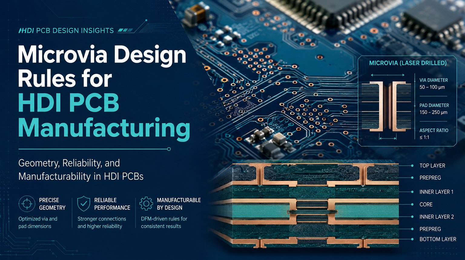
Sequentially laminated high-density interconnect (HDI) structures are more susceptible to failure due to stacked microvia fracture caused by resin recession and thinning of copper caps. Laser-drilled microvias with an aspect ratio greater than 0.8:1 can exhibit a noticeably higher crack initiation probability after thermal cycling between -40°C and +125°C.
Finite Element Analysis (FEA) can be used to predict strain energy density, via barrel deflection, and solder joint creep under designated JEDEC thermal cycling conditions. Reliability optimization can include staggered microvia architectures, low-CTE laminates below 45 ppm/°C, and balanced copper distribution to minimize warpage to less than 0.75% in large 5G backplane assemblies.
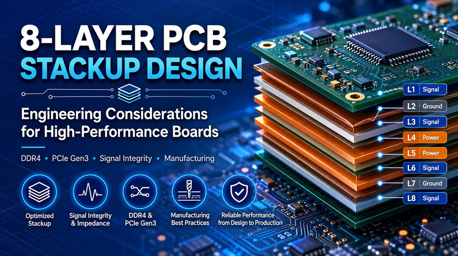
5G PCB stack-up design is not only about arranging signal, power, and ground layers. It is also used to ensure controlled impedance uniformity, reference plane continuity, and compensation for circuit board manufacturing tolerances. For example, a 50 Ω transmission line with εr = 3.45 constructed with a 0.18 mm dielectric core will shift impedance by ±2.5–3.5 Ω with a ±10 µm dielectric height and therefore affect return loss (-10 dB) at multi-GHz operating frequencies.
Warpage can be reduced through stack-up symmetry. An imbalance of copper distribution between the top and bottom layers greater than 10% will result in 0.75 mm of either bow or twist on 100 mm panels after lamination.
The sequential lamination process introduces variation in resin flow, which can result in a lateral shift of 0.20 to 0.50 mm and requires compensation with photo tool scaling and adjustment of the etch factor.
Current crowding will create higher effective resistance at high frequency, mostly due to conductor profile roughness where Rz > 2.0 µm. Therefore, simulation models should incorporate frequency-dependent surface impedance rather than relying on ideal assumptions regarding copper.
To successfully manufacture a reliable 5G PCB, electromagnetic, mechanical, and process variability design rules must be integrated at the same time.
The final validation process is complete only when the simulated S-parameters and the measured results from the fabricated board fall within the defined tolerance band.
5G PCB design is where engineering theory meets manufacturing reality. Even a well-designed RF or mmWave circuit can face performance risks if the PCB material, stack-up, impedance control, and production process are not aligned from the beginning.
PCBCool supports 5G PCB projects with both engineering review and manufacturing experience. We help customers identify design and production risks early, then turn complex high-frequency PCB requirements into reliable boards ready for assembly and real-world use.
For companies developing 5G communication equipment, RF modules, antenna systems, or other high-frequency electronic products, we can provide practical support from design discussion to PCB fabrication and assembly.