banner下面提交表单 (#30)

20+ Years of Heavy Copper PCB Experience

Among the 5,200+ projects completed at PCBCool, nearly 1/4 are related to high-current, high-power, and power distribution applications. This long-term project accumulation has enabled us to develop a systematic understanding of thermal management and current-carrying design, allowing us to quickly identify critical risk points in heavy copper PCB projects and provide targeted manufacturing and process optimization solutions.

We focus not only on manufacturing itself, but also on real-world performance and reliability. From material selection and copper thickness control to structural design optimization, we help customers reduce risks during the design phase while improving stability and consistency in manufacturing.

With continuous practice in demanding industries such as industrial and automotive, PCBCool is committed to being a trusted long-term partner, ensuring heavy copper PCB projects remain stable and efficient from development to mass production.

Heavy Copper PCB Technology Capabilities

Thick Copper PCB
Production Capabilities
SpecificationsStandardMax.
Max. Copper Thickness10oz [350µm]33oz [1155µm]
Max. PCB Size300*450mm510*620mm
Min. Trace Width / Spacing (2OZ)0.20mm / 0.18mm0.18mm / 0.16mm
Max. Board Thickness (2OZ)3.2mm6.0mm
Aspect Ratio8:110:1
Min. Hole Copper Thickness25um50um
Max. Basic Copper Thickness10oz [350µm]33oz [1155µm]
MaterialsHigh-stability Tg170 material, and PP with high Tg and high resin content
Surface FinishUsually immersion gold (ENIG)
Layout Guide
Thick Copper PCB Layout Guide
Cu ThicknessMin. Trace WidthMin. Trace SpacingMin. Spacing from Pad to TraceMin. Hole Dia.Min. Hole Annularing
2OZ0.20mm0.18mm0.16mm0.25mm0.18mm
3OZ0.30mm0.20mm0.18mm0.3mm0.18mm
4OZ0.35mm0.25mm0.23mm0.5mm0.25mm
5OZ0.40mm0.30mm0.28mm0.6mm0.30mm
6OZ0.45mm0.35mm0.33mm0.6mm0.35mm
7OZ0.50mm0.40mm0.38mm0.8mm0.40mm
8OZ0.55mm0.45mm0.43mm1.0mm0.45mm
9OZ0.60mm0.50mm0.48mm1.0mm0.50mm
10OZ0.65mm0.55mm0.53mm1.0mm0.55mm
11-33OZEvaluationNeeds Process evaluation before production
China Mainland BaseMalaysia BaseMexico Base
Turnkey ServiceDesign + PCB FAB + Components Sourcing + PCB Assembly + Product AssemblyComponents Sourcing + PCB Assembly + Product AssemblyComponents Sourcing + PCB Assembly
Assembly TechnologiesTHT, SMT, Hybrid Mount, Subsystem AssemblyTHT, SMT, Hybrid Mount, Semi AssemblyTHT, SMT, Hybrid Mount, Subsystem Assembly
Manufacturing AbilitiesPrototyping, Low to High VolumePrototyping, Low/Medium/High VolumePrototyping, Low to Medium Volume
Component AbilitiesChips 0201mm BGA, QFP & CSP 0.25mm BGA repair and reballChips 0402mm BGA, QFP & CSP 0.25mm HDMI Connectors / Micro USB ConnectorsChips 0402mm BGA, QFP & CSP 0.3mm Press Fit / High Pin Count Connectors
SMT Lines11 Lines, Samsung / JT9 Lines, Samsung / Panasonic / Sony5 Lines, Siemens / Samsung
SMT CapabilitiesMonthly 788 Million PointsMonthly 298 Million PointsMonthly 63 Million Points
THT Lines3 Lines, Auto / Manual4 Lines, Auto / Manual2 Lines, Auto / Manual
Inspection MachinesSPI, AOI, 2D X-RaySPI, Optical Measuring (VMS-4030M), X-ray (SMX-1000)SPI, AOI, X-ray, Microscope to 20X
TestingICT/Function test/Burn-in test/Aging TestingICT/Function test/Burn-in testICT/Function test/Burn-in test
Assembly CostLower CostsLower CostsMedium Cost
Lead TimeAs fast as 9 days with shippingAs fast as 7 days with shippingAs fast as 3 days with shipping
Number of layersS<1m²1≤S<5m²5≤S<20m²20≤S<50m²50≤S<100m²100m²以上Expedited (≤3㎡)
2L45-75-76-98-109-1212~24 hours
4L56-86-88-1010-1210-151~4 working days
6L66-86-88-1010-1210-152~4 working days
8L76-86-88-1010-1210-154~6 working days
10L99-119-1110-1212-1413-175~9 working days
12L1010-1210-1211-1313-1514-187~14 working days
14L1010-1210-1211-1313-1514-187~14 working days
16L111313151617Contingent
18L121414161718Contingent
20L131414161819Contingent
22L151515182022Contingent
24L151515182022Contingent
26L151515182022Contingent
28L+151515182022Contingent

Commitment to Quality

An upward pointing arrow icon

Certification Compliance Support

  • Answer Support for ISO 9001 quality management system
  • Answer Compliance with ISO 14001 environmental management system
  • Answer Adherence to ISO 45001 occupational health and safety standards
  • Answer Compliance with IPC-A-610 and IPC J-STD-001 standards
  • Answer Support for RoHS / REACH environmental compliance
  • Answer Support for UL and CE certifications
  • Answer Support for ISO 13485, IEC 62031, and other industry-specific certifications
An icon for controlling the screen

Manufacturing Process Control

  • Answer Full BOM and lot traceability across production
  • Answer Material traceability (components, boards, solder paste, etc.)
  • Answer Process documentation for regulated manufacturing
  • Answer First Article Inspection (FAI) support
  • Answer In-process quality checks and monitoring
  • Answer Controlled ESD & cleanroom processes (if applicable)
  • Answer Complete inspection records and test reports
  • Answer Change control and nonconformance management
End-to-End Solutions

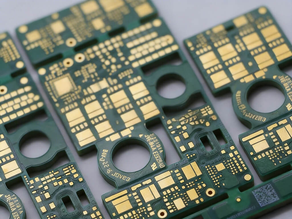
A heavy copper PCB featuring a precision circuit design

PCBCool starts with DFM evaluation and process optimization, progresses through prototyping and process validation, and ultimately delivers reliable mass production for heavy copper PCB.

  • Answer Engineering Support
  • Answer PCB Fabrication
  • Answer PCBA Assembly
  • Answer Box Build / System Integration
  • Answer Testing & Validation
  • Answer Supply Chain & Logistics
A heavy copper PCB featuring a precision circuit design
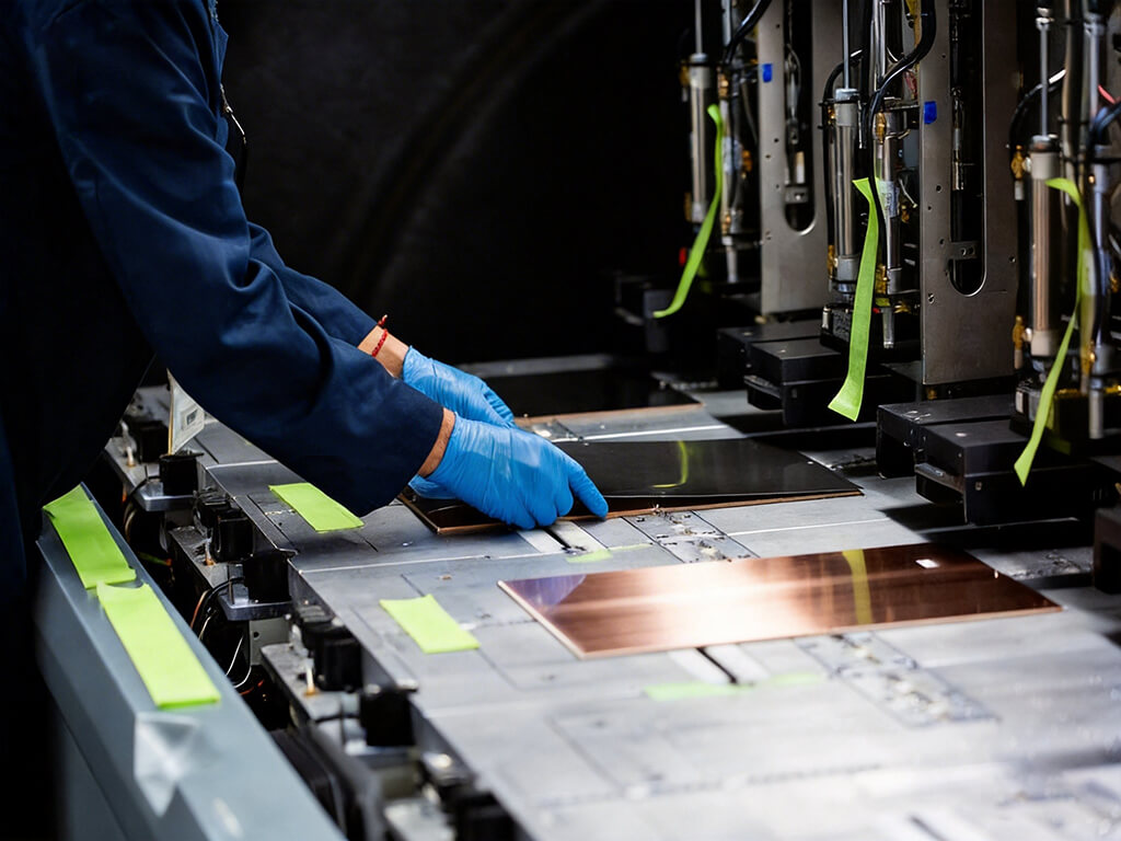
PCBCool workers are manufacturing thick copper PCB

Cutting-Edge Technologies

PCBCool workers are manufacturing thick copper PCB

PCBCool invests $200,000 annually in equipment maintenance, upgrades, and workforce training to ensure technology remains ahead of industry standards.

  • Answer Vacuum etching machine achieves ±0.015mm trace width/spacing tolerance control
  • Answer Thick copper electroplating and high-consistency copper thickness control
  • Answer Electrolytic and rolled copper foil processing technologies supported
  • Answer 12-zone reflow equipment enables precise temperature control for component soldering
  • Answer Component evaluation and replacement support for high-current and high-power applications
  • Answer PCB 220k m²/month with PCBA 15M SMT points/day

Why Choose PCBCool as Your Heavy Copper PCB Manufacturer

Heavy copper PCB manufacturing and assembly require extreme process control in etching precision, plating uniformity, and soldering stability.

If you are looking for an experienced EMS provider with advanced manufacturing capabilities —

Frequently Asked Questions

Q1: How to Evaluate Current Carrying Capability of a Heavy Copper PCB?

A: It can be estimated using IPC-2152, considering copper thickness, trace width, and allowable temperature rise. Final validation should rely on thermal simulation or testing to ensure the design meets the target temperature limit under real conditions.

Q2: How to Reduce Thermal Stress in Heavy Copper PCB Design?

A: Use gradual copper transitions, avoid abrupt thickness changes, and maintain balanced copper distribution.

Q3: How to Optimize Thermal Paths in a Heavy Copper PCB?

A: Apply large copper pours, add via arrays, and create direct thermal conduction paths.

Q4: How to Control Via Current Capacity in Heavy Copper PCB?

A: Increase via count, enlarge via diameter, and improve copper plating thickness.

Q5: How to Balance Conductivity and Impedance in Heavy Copper PCB?

A: Use heavy copper for power paths while maintaining controlled geometry for signal traces.

Q6: What are Component Selection Considerations for Heavy Copper PCB?

A: Choose components with high temperature tolerance, sufficient current rating, and strong solder joint reliability.

Q7: What Causes Redesign in Heavy Copper PCB Projects?

A: Common causes include improper copper thickness matching, insufficient via design, uneven copper distribution, poor thermal design, and lack of DFM validation.

Q8: What are Common Failure Modes in Heavy Copper PCB Thermal Cycling?

A: Common failures include via cracking, delamination, and microcracks in copper traces due to thermal expansion mismatch and repeated thermal stress.

Q9: What is the Main Manufacturing Challenge of Heavy Copper PCB?

A: The main challenge is precise copper etching and plating control. Thicker copper makes it harder to maintain accurate trace geometry and uniform copper deposition.

Q10: How does PCBCool Ensure Trace Width Stability in Heavy Copper PCB?

A: By using high-precision imaging, controlled etching processes, and strict process parameter control. DFM analysis and in-line inspection ensure consistent trace width and spacing.

Q11: How does PCBCool Ensure Via Plating Uniformity in Heavy Copper PCB?

A: By optimizing plating current distribution and using advanced electroplating processes. Cross-section analysis and X-ray inspection are used to verify plating quality.

Q12: How does PCBCool Improve Heavy Copper PCB Project Success Rate?

A: Through early DFM evaluation, design optimization suggestions, and process control from prototype to mass production, ensuring stable manufacturability and higher yield.

Q13: How does PCBCool Ensure Consistency in Heavy Copper PCB Mass Production?

A: By using standardized processes, automated production, and full inspection including AOI, X-ray, and electrical testing to maintain consistent quality.

With PCBCool, You Get More Than Assembly

you get a partner committed to zero defects, global compliance, and lasting reliability.