You may have noticed that modern electronic devices keep getting smaller while delivering the same performance—or even more. At first glance, that can seem almost counterintuitive. In reality, though, it is a natural result of advances in electronics design, and multilayer PCBs are a big part of what makes it possible. By adding conductive layers and making better use of stackup design and routing space, multilayer boards allow far more functionality to fit into the same footprint.
For electronics engineers, designing multilayer PCBs is no longer a niche skill. It has become a core part of modern board design. In this guide, we will take a close look at the key considerations involved, from stackup planning and routing strategy to power integrity, EMI control, and cost optimization.
Whether you are moving from 2-layer boards into multilayer design for the first time, or refining the layout of a high-speed board, this guide will give you a solid practical foundation for approaching multilayer PCB design with confidence.
As you know, a PCB is a bit like a sandwich, built by stacking different layers together. A multilayer PCB is simply a more complex version of that structure, with additional layers added to support more demanding electrical and mechanical requirements.
That is why stackup design is the foundation of any multilayer PCB. It determines how signals travel, how power is distributed, and how the board performs both electrically and mechanically. Get it right, and your board is far more likely to achieve strong signal integrity, stable power delivery, solid EMI performance, and good manufacturability. Get it wrong, and you may end up dealing with crosstalk, impedance issues, warping, added cost, or even rework.
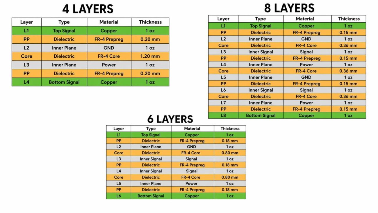
When planning a multilayer design, the number of layers is one of the first major decisions you need to make. It is always a tradeoff between performance, cost, and board size.
- 4 layers → Lower cost, easier to manufacture, and suitable for most designs, including digital, mixed-signal, and medium-speed applications.
- 6 layers → A strong choice when you need more routing space or better high-speed performance, but do not want the added cost and complexity of 8 or more layers.
- 8 to 10 layers → Often necessary for high-density, high-speed digital designs such as DDR, PCIe, multi-gigahertz systems, RF applications, or boards with very high component counts.
- 12 layers and above → Typically reserved for more demanding applications in areas such as servers, telecommunications, and advanced automotive electronics.
How do you decide?
Ask yourself:
- How many critical signals need short, clean routing paths?
- Does my board include high-speed interfaces such as USB 3.x, HDMI, or SerDes?
- How much power does the design need to carry?
- What are my target board size and budget?
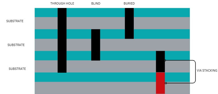
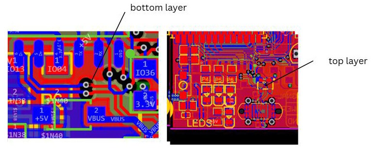
Vias are one of the key structures that make electrical interconnection between layers possible in a multilayer PCB. As layer counts increase and routing density rises, via selection becomes much more important. It directly affects signal integrity, thermal performance, space efficiency, and manufacturability.
Some people also call them thru vias or plated through-holes. Regardless of the name, they refer to vias that pass completely through the entire PCB stackup, connecting any layer to any other layer, including the top and bottom layers.
Best suited for:
- General multilayer board structures
- Simple multilayer circuit designs
- Low-cost electronic projects
- Mechanical mounting purposes
- Low-density layouts
- Power and ground distribution
- High-current traces
- Connector mounting and other mechanical attachment needs
Limitations:
- They consume routing space on every layer, even when some of those layers do not actually need the connection.
- In dense/high-layer-count boards (>10–12 layers), they waste valuable routing area and increase the risk of via stubs. (unused portions that cause signal reflections in high-speed designs >5–10 GHz).
- Aspect ratio becomes a challenge. A typical finished hole size is around 0.2 to 0.4 mm (8 to 16 mil), while board thickness is often 1.6 to 3.2 mm. That results in an aspect ratio of roughly 6:1 to 10:1. For reliable plating, keeping it at 8:1 or below is generally recommended. Once the ratio climbs above 10:1 to 12:1, the risk of poor plating, voids, and thermal cycling failures rises significantly.
- Not suitable for ultra-fine-pitch components (e.g., 0.4 mm BGA) due to space inefficiency.
A blind via connects an outer layer (top or bottom) to one or more adjacent inner layers — visible from one side only (“blind”).
A buried via connects only inner layers — completely hidden inside the board, not visible from either surface.
Best suited for:
- Freeing up outer-layer space for components and fine-pitch fanout (e.g., BGA escape).
- Reduce via stubs for better signal integrity in high-speed/RF designs.
- Enable denser layouts without increasing board size or layer count excessively.
Design guidelines:
- Blind vias: The aspect ratio (depth:diameter) is typically kept at 1:1 or below. For the best plating reliability, 0.75:1 to 0.8:1 is preferred. With mechanical drilling, the diameter generally needs to be at least equal to the depth. With laser drilling, similar to microvias, the range is often 0.6:1 to 1:1. For example, if the depth is 0.1 mm, the diameter should generally be at least 0.1 to 0.13 mm.
- Buried vias: The aspect ratio can go as high as about 10:1 to 12:1, although 8:1 to 10:1 or below is usually recommended for better plating reliability.
- Each via layer pair requires its own drill file, which usually means sequential lamination is needed.
- Size of the annular ring is typically at least 90 to 150 μm, depending on the required class and IPC-6012 requirements.
- If aspect ratio limits are exceeded, stacked or staggered structures are often used instead.
Microvias are small blind or buried vias (typically <150 μm / 6 mil diameter), typically formed by laser drilling. Under IPC definitions, a microvia is a blind structure with a maximum aspect ratio of 1:1 and a depth of no more than 0.25 mm (0.010 in.).
HDI technology uses microvias to achieve much higher routing density. Common HDI structures defined in IPC-2226 include:
- Type I: Surface microvia to the first inner layer, combined with through-hole vias
- Type II: Microvias plus buried vias plus through-hole vias
- Type III: Stacked or staggered microvias used to skip across three or more layers
Best suited for:
- Fine-pitch BGAs in the 0.4 to 0.5 mm range
- Smartphones, wearables, servers, and other highly compact products
- Escape routing under dense component fields
- Designs that need shorter electrical paths and lower inductance for better signal integrity
Design guidelines:
- The preferred aspect ratio is usually 0.75:1 to 0.8:1 for the most uniform plating.
- The practical maximum is 1:1. Beyond that point, reliability drops quickly, and issues such as voids and copper thinning at the via bottom become more likely.
- Typical dimensions are 75 to 100 μm (3 to 4 mil) drill size with pad sizes around 200 to 300 μm.
- For stacked microvias, each layer should still remain within the 1:1 aspect ratio limit. If alignment or registration is difficult, staggered microvias are generally safer.
Not every manufacturer can handle very small aspect ratios reliably. Always confirm the fabricator’s real process capability before finalizing the design.
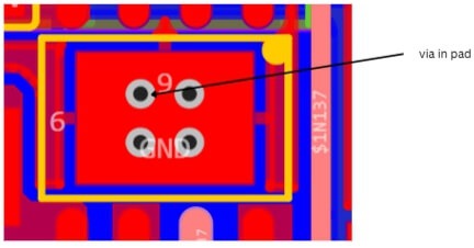
A via-in-pad, often abbreviated as VIP, is a via placed directly in a component pad, such as under a BGA or CSP solder ball.
A filled via is a via whose barrel is filled with either conductive material, such as copper-based fill, or non-conductive material, such as epoxy. It is often capped with copper plating afterward. This is commonly associated with IPC-4761 Type VI or Type VII structures.
Applications and benefits:
- Filled vias can act as thermal paths, which is useful in devices such as QFN packages and other thermally sensitive components.
- They provide lower inductance and resistance, making them more suitable for high-frequency or high-power designs.
- They allow fanout for 0.4 to 0.5 mm pitch BGA devices without needing dog-bone routing.
- They help prevent solder from wicking into the via during reflow, which improves fine-pitch assembly reliability.
- Filled vias can also reduce voiding and improve thermal cycling performance.
Design guidelines:
- The via size should remain smaller than the pad size. For example, a 0.1 to 0.2 mm drill may be placed inside a 0.3 to 0.5 mm pad.
- Non-conductive epoxy is commonly used as a lower-cost fill option, while conductive fill is used when current handling or thermal performance is more critical.
- A copper cap is required if the surface must remain solderable.
- Aspect ratio rules still apply, especially because plating must be completed before the via is filled.
It is important to confirm that the fabricator supports the relevant IPC-4761 structure. Type VII, which means filled and capped, is a common approach for via-in-pad applications.
In multilayer PCB design, impedance control is crucial for high-speed signals (>100 MHz, e.g., DDR, PCIe, USB 3.0+). Proper impedance control helps preserve signal integrity by reducing reflections, crosstalk, and electromagnetic interference. When impedance is not matched correctly, the result can be data errors, timing issues, or even complete link failure.
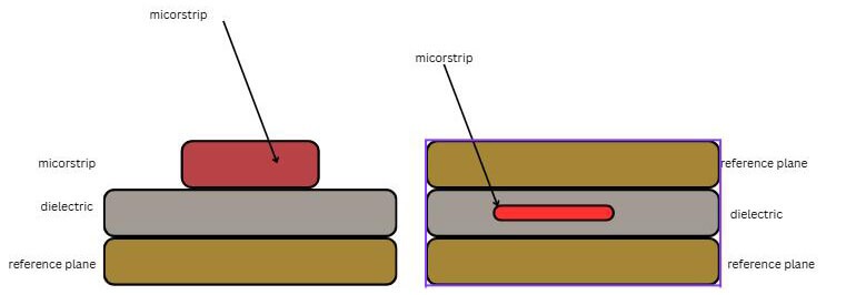
Controlled-impedance traces (e.g., 50Ω single-ended, 90–100Ω differential) behave like transmission lines. Their impedance depends on the trace geometry, the dielectric properties of the materials, and the reference plane structure.
For practical design work, engineers typically use IPC-2141 equations or field solvers such as Polar or Si8000 to estimate impedance.
For an outer-layer microstrip, the impedance can be approximated as:
Z_0 ≈ (87 / √(ε_r + 1.41)) × ln(5.98h / (0.8w + t))
where:
- h is the dielectric height to the reference plane
- w is the trace width
- t is the copper thickness (typically 0.035 mm / 1 oz)
For an inner-layer stripline, the impedance can be approximated as:
Z_0 ≈ (60 / √ε_r) × ln(1.9(2h + t) / (0.8w + t)) (Symmetric stripline between two planes.)
- Outer layers (microstrip): Exposed to air on one side (ε_r=1), so lower effective ε_r → wider traces for same Z_0. More susceptible to environmental effects (e.g., solder mask adds ~0.2–0.5 to ε_r).
- Inner layers (stripline): Sandwiched between planes → higher effective ε_r, narrower traces, better EMI shielding, but tighter tolerances due to prepreg variability.
Differential pairs (e.g., LVDS, Ethernet) carry complementary signals to improve noise immunity. When routing them across multiple layers, the main goal is to preserve tight coupling and maintain impedance balance throughout the path.
Design guidelines:
- Keep the pair spacing s less than twice the trace width w to maintain tight coupling (e.g., s=0.1–0.15 mm for 100Ω).
- Skew should generally stay below 5 to 10 ps (e.g., <1.5 mm at 3 GHz). Serpentine tuning should be done on the same layer.
- For layer transitions, use vias (blind/micro preferred) to minimize stubs (<0.5 mm).
- Stagger paired vias as needed to reduce added crosstalk.
- Differential impedance can be approximated as:
Z_diff ≈ 2 × Z_0 × (1 – k)
where k is the coupling coefficient, typically in the range of 0.1 to 0.3. Common target values fall between 90 and 120 Ω, depending on the interface standard.
- When routing across layers, ensure reference plane continuity (see below); avoid splitting pairs across asymmetric layers (e.g., microstrip to stripline shifts Z by 10–20%).
Typical applications:
- High-speed interfaces (e.g., PCIe Gen4+ at 16 GT/s) spanning 8+ layers
- Minimize via count per pair (≤2–4) to reduce discontinuities
Practical routing approach:
- Edge-coupled (side-by-side) on outer; broadside (stacked) on inner for denser packing
- In multilayer designs, route on adjacent layers if needed, but match velocities (inner slower by ~10% due to higher ε_r)
Use length tuning tools in CAD (e.g., Altium’s xSignals) for auto-matching.
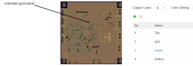
Reference planes, whether ground or power, provide the low-inductance return paths that high-speed signals depend on. Any discontinuity in that reference structure can create impedance spikes, increase EMI, and degrade overall signal quality.
Continuity rules:
- No splits under high-speed traces; use stitching vias (0.3–0.5 mm spacing) around cuts.
- Signals should have uninterrupted reference; via transitions need nearby ground vias (≤0.5 mm away) to “stitch” planes.
- Optimize h for decoupling (e.g., h<0.2 mm for <1 nH inductance).
- Avoid routing over voids or slots; if unavoidable, route orthogonally or add capacitors.
Optimization techniques:
- Via anti-pads: Size 2× drill diameter to minimize capacitance mismatch.
- Return vias: Place 1–2 per signal via in high-speed; form “via fences” for shielding.
- Power planes: Treat as reference for DC, but pair with ground for AC returns.
- Multilayer specifics: In 8+ layers, dedicate alternating signal/ground for best control.
Why this matters:
For GHz-range signals, return path quality is not optional. A poor return path can create impedance changes greater than 20 percent, which is enough to push error performance beyond acceptable limits in very high-speed systems.
A useful rule of thumb is to think in terms of current loops. Return current always tries to follow the signal path as closely as possible. If the interruption in that path becomes large enough, typically greater than one-tenth of the signal wavelength, it becomes a serious problem. At 3 GHz, that critical distance is roughly 10 mm.
DFx extends DFM/DFA/DFT for multilayers—focus on hidden features and sequential processes.
DFM (Manufacturing):
- Sequential lamination: Minimize steps (extra cost); prefer staggered over stacked vias for registration.
- Copper balance: Even distribution to avoid warpage/resin starvation.
- Fiducials: Global + local per sub-panel for inner alignment.
- HDI specifics: Aspect ≤0.8:1 for microvias; via-in-pad with fill/cap plating.
- Avoid extremes: HAR vias, ultra-thin prepregs increase yield loss.
DFA (Assembly):
- Via-in-pad: Fill + cap for planar surface (prevents solder wicking).
- Component escape: Ensure fanout accommodates blind/microvias under BGAs.
- Test points: Add accessible outer-layer points; avoid relying on inner-only features.
DFT (Test):
- Bed-of-nails: Include test vias/pads on outer; inner defects need indirect methods.
- Flying probe: Good for prototypes; add nets for continuity.
Multilayer PCB design is not just about adding more layers to a board. It is about making smarter tradeoffs between electrical performance, manufacturability, reliability, and cost. A well-designed multilayer PCB gives engineers more freedom to handle complex circuits, tighter layouts, and higher-speed requirements without losing control of the design.
At PCBCool, we support customers with multilayer PCB manufacturing and PCB assembly for a wide range of applications, from standard multilayer boards to more complex builds with tighter technical requirements. If you are working on a new multilayer PCB project and need a manufacturing partner who understands both design requirements and production realities, our team is ready to help.