High-speed PCB design used to be a specialty reserved for RF engineers and a handful of telecom hardware. That is no longer true. Modern embedded processors, communication interfaces, industrial controllers, and even consumer electronics now carry signals that switch fast enough to behave like transmission lines rather than simple copper connections.
The real dividing line is not only clock frequency. It is edge rate.
When a signal has a fast rise or fall time, it can begin reflecting from impedance changes before the transition is even complete. At that point, every millimeter of copper between the source and the load starts to matter.
This is why high-speed PCB layout should not be treated as a checklist applied after routing is finished. The rules only make sense when they are connected to one central principle:
Preserve the signal path, preserve the return path, and avoid sudden discontinuities.
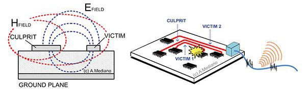
Crosstalk occurs when two nearby traces couple energy into each other through their shared electromagnetic fields. The faster the signal edge and the closer the traces, the stronger this coupling becomes.
The common 5W rule exists to reduce that risk. As a general guideline, the spacing between adjacent high-speed differential pairs should be at least five times the trace width. For example, if a controlled-impedance trace is 6 mils wide, the spacing to the next pair should be at least 30 mils.
That spacing is only the starting point.
A general keep-out of at least 30 mils should be maintained around high-speed differential traces. When a high-speed pair runs near a clock or another periodic signal, that keep-out should increase to at least 50 mils.
Clock signals are especially aggressive noise sources because they switch repeatedly at a predictable frequency. Any coupled energy can appear as a stable noise component, which makes it particularly effective at corrupting nearby signals and easy to identify later as a clean spur during spectrum analysis.
Spacing rules are not only about separating one differential pair from another. High-speed traces also need to stay away from unrelated structures and circuits that can inject noise or create discontinuities.
Probe points and test pads should not be placed directly on a high-speed differential pair. A test point creates a stub, and a stub is exactly the kind of discontinuity that can cause reflections at high-speed frequencies.
For the same reason, high-speed traces should avoid routing under or near:
- Crystals
- Oscillators
- Clock generators
- Switching regulators
- Magnetic components
- Mounting holes
- ICs that generate or distribute clock signals
These areas can introduce electromagnetic noise or disturb the local return path. A high-speed trace routed nearby can easily pick up that interference.
The area around the main chip package deserves special attention. Immediately after a BGA breakout, high-speed pairs should remain clear of the SoC package for slightly longer than a normal low-speed route would require. The current transients created by internal chip switching are strongest near the package, and once that noise couples into a nearby trace, it is difficult to remove later.
A differential pair can reject common-mode noise only when the two traces remain electrically matched. That means the pair should be routed in parallel, with consistent spacing and symmetrical geometry for as much of the run as possible.
Some deviation is unavoidable. BGA breakout regions and connector approaches rarely allow perfect parallel routing. However, these non-parallel sections should be kept as short as possible. As a practical guideline, breakout routing from the device package should be completed within about 0.25 inches of the part.
Beyond that distance, small asymmetries can begin to create measurable skew between the two halves of the pair.
Connector type also affects routing strategy.
For through-hole connectors such as a standard USB Type-A connector, high-speed pairs are often routed on the bottom layer. The through-hole pins themselves can act as stubs through the PCB, and bottom-side routing helps keep the signal path shorter and cleaner.
For surface-mount connectors such as USB Micro-B or Micro-AB, the opposite is usually preferred. Routing on the top layer allows the signal to reach the connector without an additional via transition.
The goal is the same in both cases: minimize the number of discontinuities the signal must pass through before leaving the board.
Every via is not just a connection between layers. It is a localized change in geometry, and at high-speed frequencies that geometry change behaves as both a capacitive and inductive discontinuity.
When a high-speed signal changes layers, its return current must also move between the corresponding reference planes. To keep that vertical return path short and low impedance, ground stitching vias should be placed close to the signal vias.
The most damaging part of a via is often the unused portion of the barrel. For example, if a signal moves from an outer layer to an inner layer, the remaining unused via barrel below that transition becomes a stub. That stub can behave like a small resonant structure.
Longer stubs resonate at lower frequencies and can increase insertion loss. In many high-speed designs, the unused via stub can degrade the signal more than the actual layer transition itself. This is why backdrilling is commonly used on faster interfaces to remove unused via barrel length.
SMD components placed directly in a high-speed signal path create a smaller version of the same problem. Sometimes they are necessary, such as AC coupling capacitors on high-speed interfaces. When they are required, package size matters.
As a general rule, 0603 should be treated as the largest acceptable size, while 0402 or smaller is preferred. Smaller packages introduce smaller discontinuities.
These components should also be placed symmetrically on both halves of the differential pair. If one capacitor is placed ahead of the other, the layout reintroduces skew even if the rest of the routing is carefully matched.
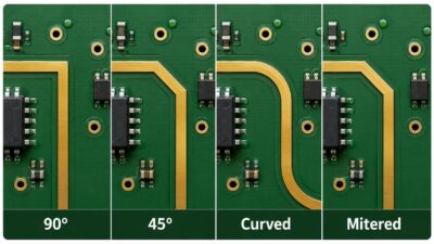
In an ideal layout, a high-speed differential pair would not bend at all. Every bend slightly changes the local electromagnetic environment, which means it also changes impedance.
When a bend is unavoidable, use a gentle 45° route or a curved trace instead of a sharp 90° corner. A gradual bend changes the current direction more smoothly and avoids concentrating the impedance change into a small area.
A sharp right angle is a small detail on the layout, but at gigahertz frequencies it can become another reflection point.
All high-speed layout rules depend on one thing: the signal must have a nearby, continuous reference plane. That means stackup planning must come before routing, not after it.
For 6-, 8-, and 10-layer boards, a good stackup keeps each high-speed signal layer close to a ground or power/ground reference plane. The exact stackup should be confirmed with the fabricator, but the design principle is consistent: do not place two high-speed signal layers directly next to each other without a reference plane between them.
Example stackup patterns:
As the layer count increases, the same logic repeats. More signal layers can be added, but each high-speed layer should still have a nearby solid reference plane.
Routing a differential pair across two stacked signal layers may look efficient, but it removes the reference plane that the signal needs. In practice, that often creates a harder signal-integrity problem than it solves.
The connector is the last point a high-speed signal reaches before leaving the PCB. It is also one of the most exposed parts of the board. That is why ESD and EMI protection components should be placed as close to the connector as physically possible.
Every millimeter between the connector and the protection device is an exposed conductor where a transient can couple into the signal before it is suppressed.
For ESD and EMI protection parts, voiding part of the reference plane under the signal pads can help reduce parasitic loading. A common approach is to void around 60% of the reference plane under those pads, depending on the device, interface, and fabricator guidance.
For common-mode filter no-stuff options, 0402 0-Ω resistors are normally preferred. A larger no-stuff component can introduce more loss than the filter position is meant to control.
AC coupling capacitors should be placed on the protected side of the common-mode filter and as close to the filter as possible. If a layer transition is required to reach the filter, the via should also be placed as close to the filter as the layout allows.
The complete protection chain — AC coupling capacitor, common-mode filter, and ESD device — should form the shortest and tightest practical cluster near the board edge.
High-speed PCB layout is not a collection of isolated rules. The 5W spacing rule cannot fix a broken reference plane. A good stackup cannot compensate for long via stubs. Perfect trace width control will not save a route that passes too close to a clock source or switching regulator.
That is why early engineering review matters. PCBCool supports high-speed PCB projects where stackup planning, controlled impedance, fabrication capability, and assembly reliability need to be considered before the board is built. If you have questions about high-speed PCB design, PCB manufacturing, or PCB assembly, feel free to contact us.