In virtually every modern electronic product, you will find at least one integrated circuit (IC) chip performing millions or even billions of operations like:
- Smartphones use chips for processing, data storage, wireless communication, imaging, audio and power management.
- Cars rely on chips for engine control, braking, navigation, safety systems and driver-assistance functions.
- Data centers, medical equipment and industrial robots all depend on the same underlying semiconductor technology.
The engineering field that makes these highly integrated chips possible is known as VLSI. However, is not simply about increasing transistor count. It is also about organizing those transistors into a useful system—one that operates at the required speed, consumes acceptable power, can be manufactured economically and continues to work reliably under real-world operating conditions.
If this is your first introduction to VLSI, this article will provide a practical starting point. It explains what VLSI means, clarifies several commonly confused concepts, and explores the internal structure of a VLSI chip.
Let us begin.
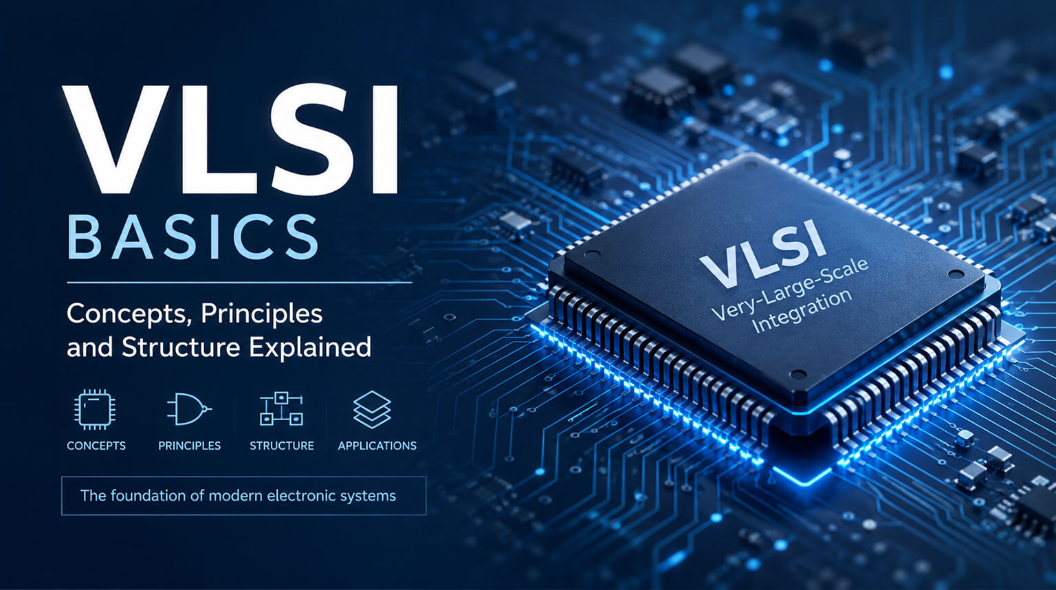
VLSI stands for Very-Large-Scale Integration, which describes a level of electronic integration in which a very large number of electronic devices and circuit components are fabricated on a single chip.
In this term:
- “Very-large-scale” refers to the number and complexity of the electronic devices integrated into the design.
- “Integration” means that transistors, interconnections and other circuit elements are manufactured together rather than assembled as separate components.
The final product is an IC chip designed for use in electronics according to the priorities of its intended application. For example:
- A mobile chip may emphasize battery life.
- A data-center accelerator may prioritize throughput.
- Automotive electronics may require strict safety and reliability measures.
- A small sensor device may need to operate for years from a limited energy source.
VLSI therefore does not refer to a specific type of chip, but rather describes a technology and engineering methodology.
Before integrated circuits became practical, electronic systems were constructed from discrete components. Each transistor, resistor and capacitor was manufactured separately and connected on a circuit board.
This approach worked for relatively simple systems, but it created several problems as circuit complexity increased:
- The equipment occupied a large physical area.
- Connections between components increased manufacturing effort.
- Long wires added electrical delay and power consumption.
- A large number of connections reduced reliability.
- Manufacturing and maintenance became expensive.
- Increasing the system’s functionality made it disproportionately more complex.
Integration changed that model. Instead of mounting and wiring individual transistors, manufacturers could fabricate many transistors and their interconnections on the same semiconductor substrate.
The advantages were significant. Integrated circuits were smaller, faster and more reliable than equivalent systems built from discrete parts. Once a manufacturing process had been established, chips could also be produced in high volumes at a comparatively low cost per device.
As integration increased, entire functions that once required multiple circuit boards could be implemented on one chip. VLSI ultimately made possible the microprocessor, high-density semiconductor memory and today’s system-on-chip devices.
The development of integrated circuits is often described using several historical levels of integration:
- Small-Scale Integration (SSI): devices contained a small number of logic gates. These chips implemented elementary functions such as inverters, AND gates, OR gates and simple flip-flops.
- Medium-Scale Integration (MSI): brought larger functions onto one device. Examples included counters, decoders, multiplexers and small arithmetic circuits.
- Large-Scale Integration (LSI): enabled considerably more complex products, including early processors and memory devices.
- Very-Large-Scale Integration (VLSI): allowed thousands, then millions and eventually billions of transistors to be integrated into highly complex circuits.
The continuing increase in integration is associated with Moore’s law:
The number of transistors per chip would grow exponentially (double every 18 months).
Semiconductor manufacturers have historically been able to increase the number of components placed economically on a chip at a rapid rate. This progress has not only made existing circuits smaller; it has allowed designers to create products with capabilities that would previously have been impractical.
Scaling has become more difficult at advanced manufacturing generations. Smaller devices intensify challenges involving leakage current, heat, process variation, interconnect delay and manufacturing cost. The industry now advances through a combination of smaller transistors, new device structures, specialized architectures, chiplets, three-dimensional integration and improved packaging.
Most digital VLSI chips process information in binary form. Voltages within the circuit represent logical values such as zero and one. Transistors control how these values are generated, stored and transferred.
A simple logic gate may require only a few transistors. A larger function requires many more. Following is a list of common functional blocks with increasing complexities inside a VLSI chip and their main use cases:
- Flip-Flop: Stores a bit of information.
- Register: Stores a group of bits.
- Adder: Performs an arithmetic operation.
- Multiplexer: Selects one input from several alternatives.
- Finite-State Machine: Controls a sequence of operations.
- Memory Array: Stores instructions or data.
- Processor: Executes instructions by coordinating datapaths, registers, memories and control logic.
Millions of these elements may operate together. Many are synchronized by one or more clock signals that determine when data is captured and when the next operation begins.
Not every circuit on a VLSI chip is digital. A device may also contain analog functions that handle continuously varying electrical signals. Modern integrated circuits frequently combine digital, analog and mixed-signal subsystems.
Most digital VLSI products are based on complementary metal-oxide-semiconductor (CMOS) technology.
CMOS circuits use two complementary types of transistors:
- n-channel MOS transistors
- p-channel MOS transistors
A CMOS inverter provides the simplest example. When the input is low, one transistor pulls the output high. When the input is high, the other transistor pulls the output low. Ideally, the circuit consumes relatively little steady-state power because there is no continuous low-resistance path between the power supply and ground.
By arranging CMOS transistors in different combinations, engineers create logic gates, storage elements and more complex circuits.
Digital designers usually do not construct every gate transistor by transistor. Instead, they use collections of pre-designed building blocks called standard cells. A standard-cell library may include:
- Buffers and inverters
- Multiplexers
- Latches and flip-flops
- Clock-gating cells
- Level shifters
- Isolation cells
- Power-switching cells
- Scan-compatible sequential cells
Each cell has known physical dimensions and electrical characteristics. Design software selects and connects these cells to implement the required functionality.
A modern VLSI product may contain far more than one processor. The exact contents depend on the application, but several types of blocks are common.
A chip may contain one or more general-purpose processor cores. It may also include specialized units for graphics, digital signal processing, artificial intelligence, image processing or cryptography. Specialized hardware can execute certain workloads faster and with less energy than a general-purpose processor. This is one reason modern chips often contain several different types of computing engines.
Processing units require instructions and data. A chip may therefore include registers, cache memories, embedded static memory, read-only memory and specialised local storage. The organization of memory strongly influences performance and power consumption. Computation may be fast, but repeatedly moving data over long distances can be expensive in both time and energy.
The blocks inside a chip must exchange information. Buses, crossbars and networks-on-chip provide communication paths among processors, memories, accelerators and peripheral controllers. As chips become larger, communication architecture becomes a major design consideration. A system with powerful processing units can still perform poorly if data cannot move among them efficiently.
Interface controllers allow the chip to communicate with memory devices, sensors, displays, networks, storage equipment and other chips. Depending on the product, these may support USB, Ethernet, PCI Express, serial links or external memory interfaces.
- Analog and Mixed-Signal Blocks
Many chips interact with the physical world through analog signals. They may include data converters, clock-generation circuits, high-speed transmitters and receivers, sensors or power-management functions.
- Security, Test and Debug Logic
Modern chips commonly include secure-boot hardware, encryption engines, diagnostic features and debug facilities. Additional circuitry is inserted so that manufacturing defects can be identified after fabrication.
The complete design of a commercial VLSI chip is a highly specialized process. For a beginner, it is useful to understand it as a sequence of connected stages.
- Define the product: Engineers begin by deciding what the chip must do. They define its functions, performance, interfaces, power limits, operating conditions and cost targets.
- Create the architecture: The system is divided into major blocks such as processors, memories, communication units and interfaces. Architects determine how these blocks will exchange data and work together.
- Describe the digital hardware: Digital designers describe the required behavior using hardware description languages such as SystemVerilog or VHDL. This description is commonly written at the register-transfer level (RTL).
- Verify the functionality: Verification engineers test whether the design follows its specification. They use simulation and other techniques to explore normal operation, error conditions and unusual combinations of events.
- Convert the design into logic gates: The logic synthesis process translates the RTL into a network of standard cells of the targeted technology.
- Create the physical layout: The cells are placed within the chip area and connected using metal wires. Separate networks distribute clocks and power throughout the design.
- Check the implementation: Engineers verify that signals arrive at the correct time, the electrical connections are correct, the power network is adequate and the physical layout follows manufacturing rules.
- Manufacture and test the chip: The completed design is sent to a semiconductor fabrication facility. The manufactured dies are tested, packaged and validated in the intended system.
In practice, this process is not entirely linear. Engineers frequently revisit earlier decisions when verification, timing, power or physical-layout problems are discovered.
The VLSI design process is commonly divided into front-end and back-end stages. Front-end design defines and verifies the chip’s architecture, logic and intended behavior, while back-end design converts that logical design into a physical layout that can be manufactured and must meet timing, power, area and reliability requirements.
Front-end VLSI focuses mainly on what the chip does. It includes:
- Architecture and microarchitecture
- RTL design
- Functional verification
- Clock and reset planning
- Design-for-test preparation
- Logic synthesis
Back-end VLSI focuses mainly on how the logical circuit is physically implemented. It includes:
- Floorplanning
- Standard-cell placement
- Power-network design
- Clock distribution
- Routing
- Timing analysis
- Power-integrity analysis
- Physical verification
Some beginners easily confuse VLSI with other related terms.
An IC is an electronic circuit fabricated on a semiconductor substrate. It is a broad term that includes both simple and highly complex chips. VLSI, by comparison, involves sophisticated engineering methods that are used to create highly complex ICs.
For this reason, every VLSI chip is an IC, but not every IC is necessarily a VLSI chip.
A simple logic-gate chip, for example, is an IC, but it may not be considered a VLSI device in the modern sense. CPUs, GPUs, high-density memory devices, and SoCs are also ICs, but they are normally designed using VLSI technology because they contain large numbers of transistors and highly complex internal structures.
The main difference therefore lies in the scale and complexity of the integration. IC is the general product category, while VLSI describes the technology and design discipline used to create highly integrated chips.
Several other related terms are commonly used in chip design:
- Application-Specific Integrated Circuit
An application-specific integrated circuit, or ASIC, is an IC designed for a defined product or purpose. A networking ASIC, for example, may be optimized specifically for packet processing.
Once an ASIC has been manufactured, its hardware structure is largely fixed. ASICs can provide high performance, low power and a low unit cost in large production volumes. Their development and manufacturing setup costs, however, can be substantial.
- Field-Programmable Gate Array
A field-programmable gate array, or FPGA, is an IC whose logic functions and internal interconnections can be configured after manufacturing.
FPGAs are commonly used for prototyping, low-volume production, and applications that may require future hardware updates. However, their flexibility comes with trade-offs.
Compared with an ASIC performing the same function, an FPGA implementation generally requires more chip area, consumes more power, and may operate at a lower maximum frequency.
A system-on-chip, or SoC, integrates multiple system functions into a single IC. The term describes how different functional blocks are combined within one chip rather than referring to a separate manufacturing technology.
An SoC may include processor cores, memory, hardware accelerators, communication controllers, peripheral interfaces, and analog or mixed-signal circuits.
VLSI makes it possible to integrate complex processing, memory and control functions into a single chip. However, a chip can only deliver value when it is correctly sourced, integrated with other components and assembled into a reliable electronic product.
PCBCool supports this process with component sourcing and PCB assembly services, helping customers move efficiently from design and prototyping to volume production.