In today’s power-hungry world, from electric vehicles and solar inverters to industrial motor drives and high-performance computing, PCBs are more than just signal carriers. They are critical power highways.
However, when currents move from a few amps to tens or even hundreds of amps, standard PCB design rules break down. If the board was not designed for high current in the first place, voltage drops will increase, heat will become destructive and reliability can be lost.
High-current PCB design is the art and science of designing boards that will safely, efficiently, and reliably deliver large amounts of power while maintaining signal integrity, thermal stability, and long-term durability. Get it right, and your product will run cooler, last longer, and perform better. Get it wrong and you will face burnt traces, delaminated boards, field failures, or even safety hazards.
This guide covers the five basic pillars of successful high-current PCB design:
- Copper Thickness – choosing the right ounce rating and understanding the manufacturing trade-offs that come with it
- Trace Widths – how to calculate the minimum widths, and why the formula is only the beginning, not the answer
- Thermal Management – why wide traces alone won’t save a high-current board, and what actually does the job
- Material Selection – matching laminate and substrate specifications to your real-world power and thermal requirements
- Component Selection – choosing power components that can handle the current and heat that your design will put on them
PCB copper thickness is measured in ounces per square foot (oz/ft²), which is the actual weight of copper that is evenly spread over one square foot of board.
Thicker copper gives you:
- Lower DC Resistance — less I²R power loss and heating
- Higher Current Capacity — carries more current without increasing trace width
- Better Thermal Spreading — heat moves laterally more easily across a thicker conductor
- Reduced Voltage Drop — critical for low-voltage, high-current rails like 12V or 48V power buses
However, thicker copper is not a “free upgrade”; it changes how the board is built, and that has real consequences for cost, lead time, and yield.
Most fabricators handle 2 oz copper comfortably, with only a small price increase over the standard 1 oz boards. Beyond that, things get harder:
Etching is essentially a “wear-away” process. Acid attacks copper from the top down and sideways simultaneously. With thick copper, the etchant takes longer to undercut the sides of a trace before it completely clears between features, forming a trapezoidal cross-section instead of a clean rectangle. The result is that your finished trace width may be very different from the designed width. The effect gets worse as the copper gets thicker.
A 1 oz layer might comfortably support 0.15 mm trace/space. If you push to 3 oz you will be looking at 0.25 mm trace or wider just to keep yields acceptable, which directly reduces how dense your routing can be.
- Drilling and Plating Challenges
Thicker copper means a larger aspect ratio between hole depth and copper height, which stresses drill bits and potentially affects via plating uniformity, especially on multilayer heavy copper stacks.
Especially in multilayer heavy copper boards, tighter control of lamination and layer registration tolerances is required. Uneven copper distribution across layers can cause warping during lamination if not balanced carefully in the layer stack-up.
- Additional Process Requirements
Fabricators usually consider 3 oz and above as “heavy copper,” which may require different etch chemistry, plating cycles or even a different production line which ultimately adds to more lead time and cost
Don’t assume “thicker is safer.” Check with your fabricator before you finalize the design. Heavy copper (3 oz+) should be a conscious decision, confirmed to be compatible with your fabricator’s process, your target trace density, and your budget, not an assumption baked in after the layout is already done.
The relationship between current, trace width, and temperature rise is governed by well-established formulas documented in IPC-2152 (the current standard) and the older IPC-2221. The idea is simple: current-carrying capacity depends on cross-sectional area. You can increase that area by widening the trace, using thicker copper, or both. IPC-2152 expresses this as:
I = k × ΔT^0.44 × A^0.725
Where:
- I = current in amps
- ΔT = allowable temperature rise above ambient (typically 10–20°C for most applications)
- A = cross-sectional area in square mils
- k = a constant, typically 0.048 for external layers and 0.024 for internal layers
Example Values (External Layer, 20°C Rise, Approximate per IPC-2152)
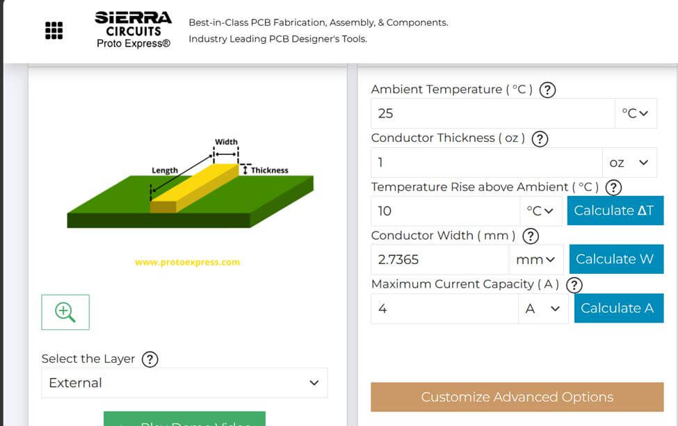
There are also online calculators that automate this; tools from Sierra Circuits and Saturn PCB are widely used. For example, for a board with -25°C ambient, 1 oz copper, a 10°C allowable temperature rise, and a maximum current of 4A, the Sierra Circuits calculator returns a required trace width of approximately 2.7365 mm.
It is easy to just plug in the numbers to IPC-2152 or an online calculator, come up with a width and then drop it into your layout and move on, but don’t. The formula gives a theoretical minimum under idealized, steady-state conditions. It doesn’t know anything about your enclosure, duty cycle, neighboring heat sources, or safety margin. Treating it as the final answer is one of the most common mistakes in high-current design. A sound decision should consider:
- Copper Thickness Interactions
The same current target will result in very different widths for 1 oz vs. 3 oz copper, and your fabricator’s actual achievable thickness after etching may be different from nominal. Do not design exactly to the calculated edge. Make sure you include a margin.
- Temperature Rise Assumptions vs. Reality
The IPC-2152 curves are for a single trace in open air on standard FR-4. If your trace runs close to other heat sources, inside a sealed enclosure, in high ambient (engine bay, outdoor cabinet) or next to other current-carrying traces, the effective rise will be higher than the chart predicts. Design for the worst-case ambient and not just the typical ambient.
- Voltage Drop, Not Just Temperature
A trace can be thermally “safe” under IPC-2152 and still cause unacceptable voltage drop on a low-voltage rail. A small IR drop in a 3.3V or 5V supply carrying 15A can push components out of spec. Calculate voltage drop (V = I × R) separately from thermal rise and size for whichever constraint is tighter.
- Thermal Dissipation of the Board
A trace does not lose heat due to its conditions alone. Thermal dissipation also depends on copper pour connectivity, board thickness, layer count, enclosure airflow, and proximity to other hot components. Identical trace widths can run at very different temperatures depending on these conditions.
- Duty Cycle and Transient Currents
Thermal behaviour of continuous and pulsed/peak currents is very different. A trace-sized for average current can still overheat under sustained peaks if thermal mass and dissipation paths are not considered.
Use IPC-2152 and calculators as a starting point, not a specification. Final trace width should combine the calculation with copper thickness realities, actual operating environment, voltage-drop, and a margin appropriate to the application.
The best high-current PCB layout tips are:
- Stitch wide traces to other copper layers with vias to share the load
- Round corners or use 45° chamfers to minimise etching defects and current crowding
- Keep high-current traces short and direct
- For currents above 50–60A, consider multiple parallel layers, copper bus bars, or heavy copper combined with copper coin technology
The more current you have, the more heat you generate and this is where many designs fail, even when copper thickness and trace width have been calculated correctly. Heat from I²R losses can still cause component degradation, trace delamination, solder joint failure, and reduced product lifespan if it has nowhere to go.
It’s an instinct to respond to a hot board by widening the trace, but widening a trace will only reduce the resistance of that trace. It does nothing to address where the heat goes once it’s generated or how its removed from the board entirely. A wide trace sitting on a thin board with no copper planes, no thermal vias and no airflow will only create a wide hot zone instead of a narrow one. The heat has to actually go somewhere, and that “somewhere” is the part of the design that trace width calculations don’t cover.
Good thermal management means the design of the entire heat path, not just the conductor generating the heat. Heat is removed through three physical mechanisms:
- Conduction — through copper planes, vias, and the board’s internal structure
- Convection — airflow across the board surface, whether natural or forced
- Radiation — a minor contributor in most PCB applications
A complete thermal strategy addresses all three. The following is the order of priority:
Use large copper pours and dedicated power/ground planes instead of relying on thin traces alone. A thicker copper (2 oz or 3 oz) will dissipate heat laterally much better than a narrow trace can. This turns a hot spot into heat distributed over a much larger area which is much easier to get rid of by convection or a heatsink.
Vias are not only used for routing signals between layers, but they are also one of the best tools to move heat vertically through the board:
- Place an array of vias directly under the thermal pad of high-power components
- Use small vias (0.3–0.5 mm diameter) on a tight pitch (1 mm or less) to maximize the number of conduction paths
- Fill or plug vias on high-power boards to improve thermal conductivity and prevent solder wicking during reflow
- Always connect thermal via arrays to large copper areas on inner or bottom layers. A via that dead-ends into a small pad accomplishes very little
- Dedicate entire layers to power and ground planes wherever the stack-up allows
- Vias can be used to stitch adjacent copper layers together to create a more continuous thermal mass through the board
- Avoid narrow thermal-relief connections on high-power pads. The same thin spokes that make hand-soldering easier also choke off the thermal and current path right where you need it most
In situations where conduction and natural convection are not enough, especially in high-power or enclosed designs, additional cooling becomes necessary. You can do this using;
- Aluminum or copper heatsinks mounted directly on high-dissipation components
- Thermal interface materials (TIMs) such as pads, paste, or phase-change materials to efficiently transfer heat between the component and heatsink
- Metal-core PCBs (MCPCB) or insulated metal substrates (IMS) for very high-power applications where the PCB itself needs to act as a heat spreader
- Forced-air cooling with fans, or liquid cooling in the most extreme, high-density power applications
Trace width handles localized resistive heating, but copper planes, thermal vias, and dedicated cooling handle getting that heat out of the board entirely. If you skip any one of these in a real high-current design, you will just be moving the failure point somewhere else
Copper thickness and trace geometry only matter if the substrate underneath can survive the thermal and electrical environment you are designing for. Standard FR4 serves many high-current boards well. But as power density increases, material specs become a real design consideration, not an afterthought.
- Glass Transition Temperature (Tg) and Decomposition Temperature (Td)
Standard FR-4 will usually have a Tg of about 130–140°C. A high-Tg laminate (170–180°C) will reduce the risk of delamination and resin softening caused by sustained thermal cycling in continuously hot running boards.
Standard FR-4 is a poor thermal conductor (roughly 0.3–0.4 W/m·K), which is exactly why copper planes and vias do most of the lateral and vertical heat-moving work. For applications where the substrate itself needs to spread heat efficiently, specialty thermally conductive laminates (1–3+ W/m·K) or metal-core constructions are worth the added cost.
- Coefficient of Thermal Expansion (CTE)
Thermal cycling repeatedly stresses plated through-holes and vias. If the CTE of the material is closer to copper, the chances of via barrel cracking over the lifetime of the product are reduced. This is especially important in automotive and industrial designs where the expected life is longer.
- Metal-Core and Insulated Metal Substrates (MCPCB/IMS)
For very high-power designs, LED arrays, high-current power supplies and motor controllers, an aluminum or copper-core substrate with a thin dielectric layer can outperform any multilayer FR-4 stack-up for heat spreading, but at the cost of routing flexibility and higher unit price.
Electrodeposited (ED) copper is a standard and cost-effective option, but rolled-annealed (RA) copper offers better ductility and is preferred for applications with significant flex or thermal cycling stresses, such as automotive underhood electronics.
| Application Profile | Recommended Material Direction |
|---|
| General high-current design, moderate duty cycle, benign environment | Standard FR-4, Tg ~140°C, 2 oz copper |
| Continuous high power, elevated ambient, industrial/automotive applications | High-Tg FR-4 (170°C+), consider thermally conductive laminate |
| Very high power density, LED, or compact power modules | MCPCB / IMS substrate with aluminum or copper core |
| Long-life automotive or harsh thermal-cycling environments | High-Tg, CTE-matched laminate, RA copper foil |
The right material choice depends on duty cycle, ambient temperature, expected service life, and power density, not just peak current. Specifying material properties alongside copper weight and trace geometry rather than defaulting to generic FR4 is often the difference between a board that survives qualification testing and one that doesn’t.
Even a perfectly designed copper and thermal structure can be undermined by underrated components. Consider these parameters for the key power-handling parts in your design:
Choose low RDS(on) to minimize conduction losses. Look for packages with exposed thermal pads (PowerPAK, TO-Leadless, DirectFET, LFPAK). Check the Safe Operating Area (SOA) and avalanche rating, and choose 40V–60V parts for 12V–48V systems to keep voltage headroom.
Saturation current (Isat) must exceed your peak current, not just average current. Check the RMS current rating and temperature-rise curves, use shielded types in EMI-sensitive designs, and favor low DCR parts to minimize losses.
Input capacitors need a high ripple-current rating and low ESR. Output capacitors need sufficient capacitance plus low ESR/ESL for loop stability. Polymer types, MLCC arrays, or electrolytics with high ripple-current specs are generally the best fit.
Rate for your maximum current plus a 20–50% margin. High-current connectors (Molex, Anderson Powerpole, screw terminals) often require derating at elevated ambient temperatures, so pay close attention to contact resistance and the temperature rise it causes under sustained load.
Use Schottky diodes for low forward-voltage drop in switching applications. Ensure adequate current and thermal ratings, including surge conditions.
High-current PCB design is not solved by choosing a wider trace or thicker copper alone. The real challenge is making sure the electrical, thermal, and manufacturing decisions work together before the first board is built.
A design that looks acceptable in a calculator may still fail when it enters real conditions: limited airflow, continuous load, manufacturing tolerances, or long-term thermal cycling. This is why high-current projects benefit from early collaboration between designers and PCB manufacturers.
At PCBCool, we help engineers review high-current PCB requirements from both design and manufacturing perspectives, including copper weight selection, heavy copper capability, thermal considerations, stack-up planning, and production feasibility. By addressing these factors before fabrication, potential reliability issues can be identified earlier and unnecessary redesigns can be avoided.
A reliable high-current PCB is not created by one parameter. It is created when the design intent, material selection, and manufacturing process are aligned from the beginning.