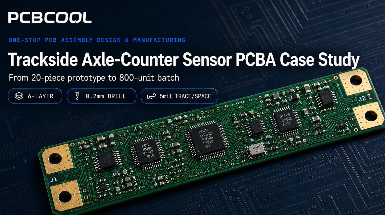
In a railway signalling system, an axle counter uses trackside sensors to detect passing wheels and help determine whether a section of track is occupied or clear. The PCBA in this project sits at the front end of that process, where reliable wheel detection and signal processing are essential.
PCBCool recently worked on a trackside wheel-detection sensor PCBA for this type of axle-counting system. We selected the project as a representative case study to show how it progressed from prototype development to the subsequent production program.
Note: This case study is published with the customer’s permission and was reviewed by the customer before publication.
The customer is an independent European subsidiary of a global rail technology group founded in 1938, with more than 50,000 employees worldwide. The group supplies railway infrastructure and signalling equipment, including axle-counting systems, track circuits, railway signals, and point-control systems, to major rail operators across Europe.
For this project, the customer selected PCBCool’s turnkey service. The cooperation began with 20 assembled prototypes and later expanded into a rolling program of 800 PCBAs, covering eight related board variants used within the same signalling system.
| Parameter | Specification |
|---|
| PCB Design | 6-layer PCB designed in Cadence Allegro 25.1 |
| Board Format | Long, narrow trackside sensor board with terminal pads at both ends |
| Base Material | High-Tg FR-4, Tg ≥170°C |
| Finished Thickness | 1.6 mm typical |
| Copper Weight | 1 oz outer layers; 0.5–1 oz inner layers |
| Surface Finish | ENIG |
| Minimum Trace / Space | 5 mil / 5 mil (0.127 mm) |
| Minimum Drill Size | 0.2 mm |
| Drill Tolerance | ±0.05 mm |
| Special Processes | Via-in-pad and impedance control |
| Standard | Application |
|---|
| EN 50125 | Environmental conditions for railway equipment |
| EN 50121 | Railway electromagnetic compatibility requirements |
| EN 50155 | Electronic equipment requirements used as a project design reference |
| Function | Component |
|---|
| MCU | ST STM32U073RCI6 |
| Buck Converter | TI TPS62840DLC |
| Magnetic Sensor | TI TMAG5173A2-Q1 3D Hall-effect sensor |
| Temperature and Humidity Sensor | TI HDC3022QDEFRQ1 |
| Level Translator | TI TXU0104RUTR 4-bit level translator |
| Circuit Protection | Littelfuse SC3051-04HTG TVS array |
| Clock | Abracon 32.768 kHz crystal |
| Capacitors | Murata 4.7 µF, 10 µF, and 100 nF capacitors |
| Inductor | 2.2 µH inductor |
| Resistors | Vishay resistors |
| BOM Size | 16 line items |
| Parameter |
Requirement |
| Component Sourcing |
100% turnkey component sourcing |
| Assembly Process |
SMT assembly, including BGA, QFN, and other leadless packages |
| Protective Coating |
Conformal coating for trackside environmental protection |
| Connector Assembly |
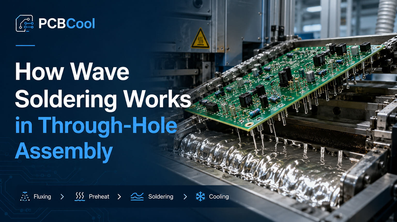
Selective wave soldering for through-hole connectors |
| Inspection |
AOI and X-ray inspection |
| Testing |
Electrical testing before shipment |
The difficulty of this project did not come from one technical specification alone, but from several constraints occurring at the same time.
The board used a 6-layer construction with via-in-pad structures and 5 mil trace and space. Together, these features required a level of process control approaching HDI production and increased the manufacturing risk. Because some vias were located directly within component pads, any solder loss into the via or unevenness on the pad surface could affect component seating and solder-joint consistency. With an initial order of only 20 boards, there was also little yield buffer.
The 16-line BOM added a separate sourcing challenge. It included automotive-qualified sensors and several components with limited or uncertain availability. Every part had to match the approved specification, remain traceable, and arrive in time for assembly. Component procurement was therefore not a separate administrative task; it became part of the production schedule itself.
The prototypes also had to arrive within the customer’s fixed commissioning window. Short-notice, low-volume projects often face longer lead times and small-batch premiums, especially when PCB fabrication and assembly are handled by different suppliers.
This was the model the customer was really testing:
Whether one partner could manage high-reliability manufacturing, low-volume production, and fast turnaround without dividing PCB fabrication and assembly between separate vendors.
After reviewing these challenges, our engineering team adopted the following measures:
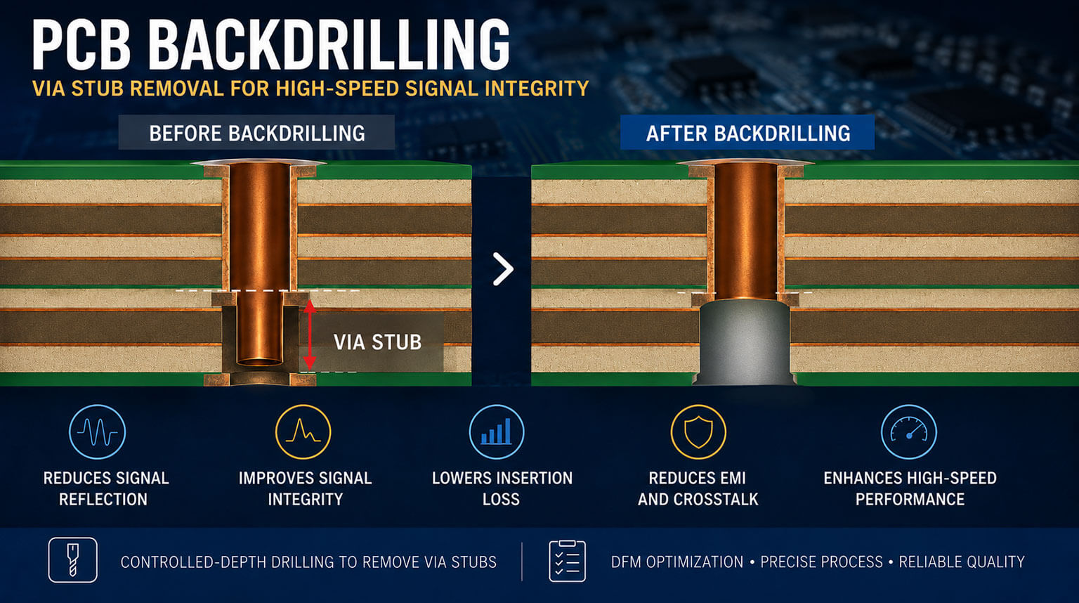
The vias located within component pads were filled, planarized, and plated over. Filling closed the path that could otherwise draw solder into the hole during reflow soldering, while planarization and plating restored a flat surface for component soldering.
Direct imaging was used for the 5 mil trace-and-space pattern instead of conventional film exposure, reducing registration variation caused by phototool movement or dimensional change. Vacuum-assisted etching improved the circulation of etchant across the panel and reduced solution pooling, helping maintain the intended conductor width and spacing.
All 16 BOM line items were sourced through authorized, traceable channels and checked against the approved manufacturer part numbers and package specifications. Procurement started alongside PCB fabrication so that component availability would not hold back the assembly schedule.
The board combined fine-pitch leadless devices in the central sensor area with large terminal pads at both ends. Placement and reflow settings were therefore planned to accommodate both component types within the same production flow. Once assembly was complete, the boards moved directly into inspection and testing without being transferred to a separate supplier.
Quality checks were carried out at each stage of the project rather than only after assembly:
| Gate | Focus | Key Checks |
|---|
| IQC | Materials and components | - Laminate verification;
- Authorized-channel components with lot traceability;
- Automotive-qualified ICs verified against manufacturer lot data.
|
| IPQC | Fabrication and assembly | - Via-in-pad fill quality;
- DI registration for 5 mil features;
- Reflow profile verification.
|
| OQC | Finished PCBA | - Electrical testing;
- AOI inspection;
- X-ray inspection.
|
For this project, X-ray inspection was mandatory because the solder joints of the leadless components were hidden beneath the package.
The 20-piece prototype did more than prove that the board could be built. It showed that PCBCool could manage the project reliably enough to earn the customer’s continued trust and follow-on work.
If you are looking for a true manufacturing partner—not just a supplier for a single order—consider PCBCool for support from prototype development through repeat production.