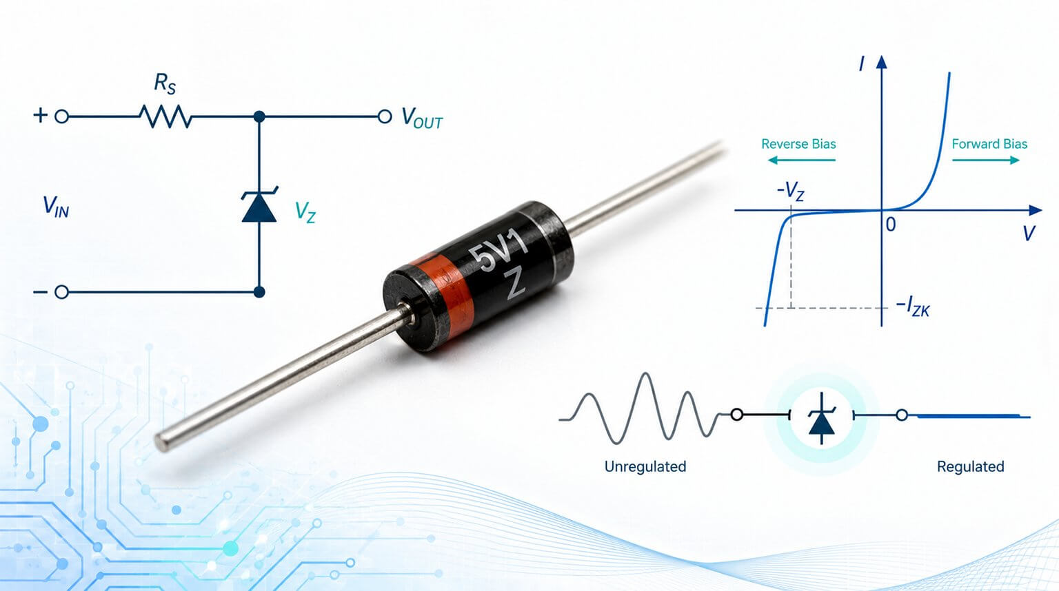
There are different diode types and each is designed to accomplish different purposes in circuit applications; for instance, rectifier diodes are used to convert AC mains voltage to DC and TVS diodes are used for surge and ESD protection.
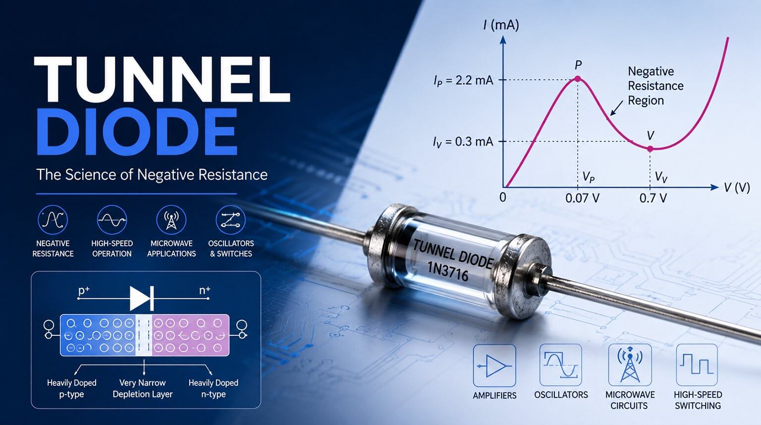
Conventional diodes usually exhibit positive resistance when they are forward-biased (i.e., current flowing through a circuit increases as the voltage is increased). On the other hand, a tunnel diode exhibits negative resistance between two values of forward voltage; in other words, current decreases as the voltage is increased in certain regions in the forward direction. This makes tunnel diode a preferred choice in applications such as high-speed switching circuits.
In this article, we will explain the principal details and operation as well as applications of tunnel diodes, giving you the foundational knowledge you need as an engineer designing systems that incorporate tunnel diodes or educating you as an enthusiastic electronics learner who is just getting started learning about them.
Let’s go straight to it.
A tunnel diode, also referred to as an Esaki diode, is a semiconductor p-n junction diode that exhibits negative resistance between two values of forward voltage, that is, between peak-point voltage and valley-point voltage.
A typical semiconductor diode usually exhibits positive resistance when it is forward-biased, but if a semiconductor junction diode is heavily doped with impurities, it exhibits negative resistance (i.e., current decreases as the voltage is increased) in certain regions in the forward direction – this is a key characteristic feature of a tunnel diode.
This unique property of tunnel diodes arises from quantum tunneling and makes tunnel diodes especially valuable in microwave and high-frequency applications where it can act as an amplifier, oscillator, and high-speed switch.
Essentially, the tunnel diode is still a p-n junction but with heavy doping of p-type and n-type semiconductor materials. As a matter of fact, a tunnel diode is doped approximately 1000 times as heavily as a conventional diode.
The heavy doping in a tunnel diode gives rise to a large number of majority carriers. Because of the large number of carriers, most are not used during the initial recombination that produces the depletion layer. Consequently, the depletion layer is very narrow.
This very narrow depletion layer is what makes the tunneling effect possible. Tunneling can be defined as the movement of valence electrons from the valence energy band to the conduction band with little or no applied forward voltage. In other words, we can say that the valence electrons seem to tunnel through the forbidden energy band.
Because the depletion layer is extremely narrow, it takes only a very small applied forward voltage to cause conduction. As the forward voltage increases through a certain range, the tunneling current first increases and then decreases, forming the negative resistance region that makes the tunnel diode different from ordinary diodes.
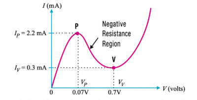
When a small forward bias voltage is applied across a tunnel diode, it begins to conduct current. As the voltage is increased, the current increases and reaches a peak value called the peak current (IP = 2.2 mA) at about peak-point voltage VP (=0.07 V). Up to this point, the diode has exhibited positive resistance.
If the voltage is increased a little more, beyond VP, the current actually begins to decrease until it reaches a low point called the valley current (IV = 0.3 mA) and where the valley-point voltage (Vv = 0.7 V).
In the region between peak-point and valley-point, that is, between points P and V, the diode exhibits negative resistance, that is, as the forward bias voltage is increased, the current decreases. This suggests that the tunnel diode, if operated in the negative resistance region, can be used as an oscillator or a switch.
If the voltage is increased further beyond the VV = 0.7 V, the current begins to increase again, this time without decreasing into another ‘valley’; in other words, from point V onwards, the tunnel diode behaves as a normal diode, i.e., the diode exhibits positive resistance once again.
Note that the tunnel diode usually has a high reverse current but operation under this condition is not normally used.
The forward voltages necessary to drive a tunnel diode to its peak and valley currents are known as peak voltage VP and valley voltage VV respectively. The region on the graph where current is decreasing while applied voltage is increasing, that is, between VP and VV on the horizontal scale, is known as the region of negative resistance.
Tunnel diodes are able to transition between peak and valley current levels very fast, switching between high and low states of conduction much faster than even Schottky diodes. Tunnel diode characteristics are also relatively unaffected by changes in temperature.
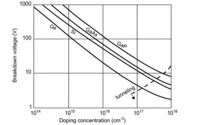
Tunnel diodes are heavily doped in both P and N regions, 1000 times the level in a conventional rectifier diode. This has been illustrated in the figure below:
Referring to the figure above, you can observe the reverse breakdown voltages versus various doping concentration levels for standard diodes, Zener diodes and tunnel diodes. The standard diodes are to the far left, the Zener diode near the left, and tunnel diodes to the right of the dashed line.
The heavy doping produces an oddly thin depletion region. This, in turn, produces an unusually low reverse breakdown voltage with high leakage. The thin depletion region causes high capacitance. To overcome this, the tunnel diode junction area must be tiny.
The forward diode characteristics consist of two regions: a normal forward diode characteristic with the current rising exponentially beyond VF, 0.3 V for germanium and 0.7 V for silicon semiconductor materials.
In reference to the figure above: between 0 and VF is a ‘negative resistance’ characteristic peak. This occurrence is due to the quantum mechanical tunneling involving the dual particle-wave nature of electrons.
In tunnel diodes the depletion region is thin enough compared with the equivalent wavelength of the electron that they can tunnel through. Thus, tunnel diodes do not have to overcome the normal forward diode voltage VF.
The negative portion of the curve can be explained as follows:
The energy level of the conduction band of the n-type semiconductor material overlaps the level of the valence band in the p-type semiconductor region. With increasing voltage, tunneling begins; the levels overlap and current increases, up to a point. As the current increases further, the energy levels overlap less; the current decreases with increasing voltage. This is the ‘negative resistance’ portion of the curve.
Tunnel diode applications include:
- High-frequency oscillators and amplifiers due to their very fast tunneling response.
- Microwave and terahertz generators.
- High-speed switching, memory and logic elements in niche and legacy designs.
- Frequency converters and mixers.
Note that tunnel diodes are not a good choice as rectifier diodes, as they have relatively high leakage current when reverse-biased. As a result, they find application only in special circuits where their unique tunneling effect has value.
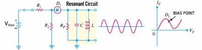
To make the most of the tunnel effect, these diodes are maintained at a bias voltage somewhere between the peak and the valley voltage levels, always in a forward-bias polarity (anode positive, and cathode negative).
Maybe the most common application of a tunnel diode is in simple high-frequency oscillator circuits, where it allows a DC voltage source to contribute power to a resonant circuit, the diode conducting when the voltage across it reaches the peak (tunnel) level and effectively insulating at all other voltages. The resistors bias the tunnel diode at a few tenths of a volt centered on the negative resistance portion of the characteristic curve. The resonant/LC circuit may be a section of waveguide for microwave operation. Oscillation to 5 GHz is possible.
A tunnel diode is always operated in the negative resistance region. When operated in this region, it works very well in an oscillator.
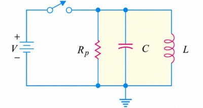
Let’s consider the resonant circuit below for our discussion here:
Notice that RP is the parallel equivalent of the series winding resistance of the coil.
When the resonant circuit is set into oscillations by applying voltage as illustrated in the circuit below, damped oscillations are produced. This is because energy is lost in the resistance RP of the resonant circuit.
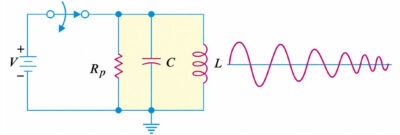
If we place a tunnel diode in series with the resonant circuit and biased at the center of the negative resistance portion of its characteristic as shown in the circuit below, undamped oscillations are produced at the output. This is due to the fact that the negative resistance characteristic of the tunnel diode counteracts the positive resistance characteristic of the resonant circuit.
The circuit above is termed a tunnel diode oscillator or negative resistance oscillator.
The negative resistance oscillator has one key shortcoming: While the circuit works very well at extremely high frequency (upper megahertz range), it cannot be used efficiently at low frequencies. Generally, low-frequency oscillators utilize transistors.
Tunnel diodes are the preferred choice in some applications because:
- They are extremely fast (i.e., sub-nanosecond) switching due to tunneling (no carrier transit delay).
Tunnel diodes are limited in several ways:
- They operate at very low voltages.
- They have limited output power and small signal levels.
- They face manufacturing reproducibility challenges – they have largely been replaced in many roles by modern semiconductor devices; however, you may still find them in use in specialized high-speed or microwave applications.
- Competition from advanced CMOS, III-V HEMTs, graphene and plasmonic THz devices and superconducting circuits for some cryogenic uses. These make tunnel diodes unlikely to replace mainstream transistors.
Tunnel diodes (both resonant tunneling diodes and newer variants like asymmetric space tunnel [ASPAT] – a variant of tunnel/Esaki-style diodes that are engineered to produce useful rectification or detection at high frequencies while minimizing DC offset and improving responsiveness) are likely to remain niche as vital components for ultra-high-frequency and quantum/cryogenic electronics rather than returning to mainstream CMOS logic.
Here are the reasons why tunnel diodes are here to stay:
- Their strengths make them not an easy replacement in specific applications: tunnel diodes possess extremely fast quantum tunneling switching and intrinsic negative differential resistance (which is useful for oscillators, mixers, detectors), additionally, their good performance at microwave – THz frequency levels and use at cryogenic temperatures for quantum readout.
- There are active research directions for tunnel diodes: III-V heterostructures (InGaAs/AIAs RTDs), asymmetric space devices (ASPAT/QASPAT) for THz-level detectors/oscillators, silicon-compatible tunneling approaches for low-power integration and device/circuit co-design for enhanced PVCR and output power.
The near-term outlook say, 5 years for tunnel looks positive, driven mainly by:
- Growth in specialized THz sources, detectors, and ultra-fast analog components for communications, sensing and imaging.
- There is more integration with III-V photonics and heterogeneous silicon processes for niche-on-chip functions such as clocking.
The longer-term outlook (10+ years) for tunnel diodes also looks good as there is continued niche adoption for terahertz (THz) electronics, cryogenic classical/quantum control, and ultrafast mixed-signal blocks where their extreme speed or negative differential resistance (NDR) in their current-voltage characteristics is uniquely valuable.
Additionally, their wider use depends on breakthroughs raising PVCR (Peak-to-Valley Current Ratio) and output power, or on application shifts, for example, THz wireless, advanced imaging or cryogenic-electronics scaling.
Higher PVCR (= Ip/IV) improves oscillator stability gain in negative differential resistance (NDR) amplifiers, switching margin in logic/memory uses, and detector linearity; low PVCR limits output power and circuit performance. For practical RTD/ASPAT applications, PVCR values of levels (e.g., 3-10+) are very desirable; research aims to increase PVCR while keeping low VP and sufficient IP.
A tunnel diode is a small device, but it shows how much circuit performance can depend on choosing the right semiconductor component. In real electronic design and production, understanding how a component works is only the first step. Engineers also need to consider availability, package options, equivalent parts, long-term supply, and whether the selected component can be reliably sourced for prototype and mass production.
At PCBCool, we support PCB assembly projects with component sourcing services to help customers simplify this process. From standard components to project-specific parts, our team can assist with BOM review, component procurement, alternative part suggestions, and supply chain coordination, helping your PCB and PCBA projects move from design to production more smoothly.