BGA, short for Ball Grid Array, is a package format that places solder balls across the bottom of the package rather than leads around the perimeter. That change may look simple on the surface, but it has major implications for I/O density, signal integrity, thermal behavior, PCB routing, assembly yield, and long-term reliability.
Compared with leaded packages such as QFP, a BGA can support more connections in a given footprint while shortening the electrical path between the die and the board. That is one reason BGA became the default direction for processors, memory devices, ASICs, FPGAs, and many high-density control devices.
But “BGA” is not one package. It is a broad family. Different BGA types use different substrate materials, die interconnect methods, package heights, pitches, and structural priorities. Some are built for mainstream volume manufacturing. Some are optimized for thin mobile products. Others exist because organic substrates are not reliable enough for the intended environment.
This article looks at the main BGA package types from a practical engineering standpoint: what they are, where they make sense, and what they change in design, assembly, inspection, and production.
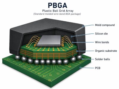
PBGA stands for Plastic Ball Grid Array. It is one of the most common organic-substrate BGA formats. In a typical PBGA structure, the die is attached to an organic laminate substrate, connected through wire bonding, overmolded with plastic compound, and finished with a solder ball array on the bottom.
In practical terms, PBGA is the standard “general-purpose” BGA platform for medium to fairly high pin-count devices. It is not the most aggressive package in the market, but it covers a wide middle ground very well.
Typical PBGA package sizes often fall in the teens to low-30 mm range, common ball pitches are 0.8 mm and 1.0 mm, and ball counts can range from a few hundred to close to 1,000, depending on the device and substrate design.
PBGA remains common because it balances several things well at the same time: package density, cost, supply chain maturity, and SMT manufacturability. It fills the gap between leaded packages that run out of room and higher-end packages that drive up substrate complexity and total system cost.
For many MCUs, DSPs, ASICs, graphics chipsets, memory devices, and mid-range processors, PBGA provides enough I/O density without forcing the board into extreme HDI territory. A 0.8 mm or 1.0 mm pitch package is still challenging at higher ball counts, but it is usually far more manageable than the finer-pitch options used in compact mobile products or high-end flip-chip devices.
PBGA’s weakness is not that it is hard to build. The real issue is that it has practical ceilings.
The first is moisture sensitivity. PBGA is a non-hermetic plastic package, so floor life matters. If handling and bake control are poor, trapped moisture can expand during reflow and cause delamination or internal cracking—the classic “popcorn” failure mode. That is a very real production risk, especially in volume assembly.
The second is electrical and thermal headroom. Most traditional PBGAs rely on wire bonding. That means the signal path from die to substrate is longer than in a flip-chip structure, which increases parasitic inductance and makes PBGA less attractive for very high-speed interfaces, very high I/O counts, or chips with dense power delivery demands.
PBGA is a good fit for projects that want a proven package with broad manufacturing support and reasonable board-level demands. It commonly shows up in:
- MCUs and embedded processors
- DSPs and mid-range ASICs
- memory devices
- graphics and PC support chipsets
- industrial control boards
- communication modules with moderate complexity
The reason PBGA works in these products is not just “it is widely used.” It works because the package is mature, the assembly flow is familiar, and the board requirements stay within a range that many volume manufacturers can support without pushing cost too far.
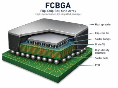
FCBGA stands for Flip-Chip Ball Grid Array. The defining difference between FCBGA and PBGA is the die-to-substrate connection method. PBGA typically uses wire bonds. FCBGA flips the die face-down and connects it to the substrate through solder bumps or similar direct interconnect structures.
That structural change matters. A flip-chip interconnect is dramatically shorter than a wire-bond path, which reduces parasitic inductance and improves high-speed electrical behavior. It also frees up more of the package surface for dense I/O distribution and power-ground network design.
Most FCBGA packages are built on advanced laminate substrates, though ceramic-based versions also exist in some high-end cases. These substrates often use multi-layer routing, microvias, blind/buried vias, stacked vias, and very fine trace/space geometries to support the package density.
FCBGA is the package of choice when the chip itself demands more than a conventional wire-bond BGA can reasonably deliver. That usually means some combination of:
- very high I/O count
- high-speed serial interfaces
- dense power and ground distribution
- large die size
- high thermal density
This is why FCBGA is common for CPUs, GPUs, high-end FPGAs, networking ASICs, AI accelerators, and other compute-heavy devices.
Its thermal advantage also comes from structure, not marketing language. Many high-end FCBGA devices include an integrated heat spreader or lid, which gives heat a more efficient path away from the die and into the system cooling solution. In a mainstream molded package, much of the thermal burden still has to spread through the substrate and board. In an FCBGA with a lid, the package is often designed from the start to work with a heatsink, cold plate, or other system-level cooling hardware.
FCBGA is not just a better PBGA. It changes the board and manufacturing equation.
First, the substrate is far more demanding. Fine-pitch, high-ball-count FCBGA packages require advanced substrate technology, and that complexity carries through to the PCB. Escape routing becomes harder, stack-up planning gets tighter, impedance control becomes less forgiving, and HDI features often move from optional to necessary.
Second, the assembly window narrows. As pitch decreases and package size increases, warpage control, coplanarity, stencil design, paste volume, reflow consistency, and X-ray inspection all become more critical. Rework is possible, but the practical question is often whether post-rework reliability is still acceptable, especially with large body sizes or lidded packages.
Third, the supply chain is tighter and more expensive. A lot of the value in FCBGA comes from advanced substrate capability, and that part of the packaging ecosystem has been one of the industry’s bottlenecks for years. So once a design commits to FCBGA, the package choice usually affects much more than the package itself. It affects sourcing strategy, cost structure, lead time risk, and manufacturing flexibility.
FCBGA belongs in systems where performance requirements are already pushing beyond the comfortable range of standard organic BGAs. Typical examples include:
- server and data center processors
- GPUs and accelerator cards
- advanced FPGAs
- networking and switch silicon
- complex industrial compute platforms
- high-end embedded systems with dense I/O and fast interfaces
If PBGA is the package you choose when you want a mature, cost-aware solution, FCBGA is the package you choose when the silicon no longer gives you that option.
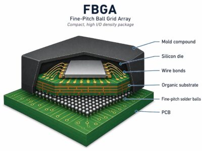
FBGA means Fine-Pitch Ball Grid Array. It is better understood as a geometry-driven BGA class than as a completely separate material family. In other words, the key feature is the tighter ball pitch, not some entirely different packaging platform.
Compared with a conventional 0.8 mm or 1.0 mm pitch BGA, FBGA typically moves into 0.65 mm, 0.5 mm, 0.4 mm, and sometimes tighter ranges, depending on the device category. That lets manufacturers fit more I/O into a smaller package outline or reduce package size without giving up the needed connections.
FBGA makes sense when board area is limited but the product still needs more interconnect density than a leaded or larger-pitch package can provide. That is why FBGA is common in compact consumer and portable electronics, especially where every few square millimeters of board area matter.
It is often used for:
- memory devices
- application processors and companion ICs
- RF and connectivity devices
- PMICs and interface ICs
- compact SoCs and support chips
The reason is straightforward: FBGA pushes package density without necessarily stepping all the way into premium flip-chip or wafer-level territory.
The package gets smaller, but the board gets harder.
Once pitch drops into the 0.5 mm and 0.4 mm range, escape routing becomes much more demanding. Fan-out strategies get tighter, via choices become more constrained, and HDI features may be required sooner than a designer would prefer. What looks like a package-space win on the component side often becomes a routing and fabrication challenge on the PCB side.
Assembly tolerance also tightens. Fine-pitch solder balls leave less room for paste variation, placement offset, bridging control, and reflow inconsistency. X-ray inspection becomes more important because the margin for hidden defects is smaller. Rework is still possible in many cases, but the process becomes less forgiving as pitch shrinks.
FBGA is a practical choice when the product needs compact packaging but does not need the full electrical and thermal performance of a high-end FCBGA. It fits well in:
- smartphones and tablets
- wearable electronics
- portable medical devices
- compact communication modules
- high-density embedded modules
- memory-heavy consumer boards
Its value is not that it is “advanced.” Its value is that it compresses package size and I/O density in a way that many mass-market products can still absorb.
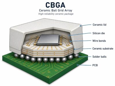
CBGA stands for Ceramic Ball Grid Array. Instead of an organic laminate substrate, it uses a ceramic package body or ceramic substrate. That changes the material behavior in important ways. Ceramic offers stronger dimensional stability over temperature, good resistance to harsh environments, and a reliability profile that can be attractive in long-life systems.
CBGA is not a low-cost or mainstream volume package. It exists because some applications care less about aggressive miniaturization and more about long-term stability under demanding operating conditions.
The reason to choose CBGA is not package density. It is reliability under stress.
Ceramic materials generally handle wide temperature swings, long service life, and mechanically or environmentally demanding conditions better than standard organic laminate packages. In systems exposed to repeated thermal cycling, the dimensional stability of the package can matter as much as the electrical performance of the die.
That is why CBGA shows up more often in areas such as:
- aerospace electronics
- defense systems
- certain high-reliability industrial controls
- long-life communication or control hardware in harsh environments
CBGA solves reliability problems by introducing cost and manufacturing constraints.
Ceramic-based packages are typically more expensive to process and source than organic alternatives. They also do not align particularly well with cost-sensitive, high-turn consumer production models. If a project chooses CBGA, it is usually because the system requirements justify a higher packaging burden.
In other words, CBGA is not an upgrade in the everyday sense. It is a deliberate move toward a higher-reliability packaging strategy for systems that cannot afford the risk profile of a mainstream organic BGA.
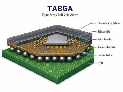
TABGA stands for Tape Array BGA. Instead of using a rigid laminate substrate like PBGA, it relies on a flexible tape or thin polymer-based interconnect structure. The goal is not maximum performance. The goal is a lower-profile, lighter package.
TABGA is best understood as a form-factor-driven package style. It is used when package thickness and weight matter more than pushing I/O count or thermal dissipation as far as possible.
TABGA makes sense in designs where the package must stay thin and light, and where the electrical and thermal demands remain within a moderate range. That can matter in certain portable products, legacy mobile designs, or special modules with strict height limits.
The same thin, flexible structure that makes TABGA attractive in some designs also creates limits.
Because the package is less rigid, it tends to be more sensitive to warpage, local stress, and solder joint reliability under assembly and thermal cycling. It is also not the natural choice for high-power devices or packages with very large I/O counts. Compared with rigid organic-substrate BGAs, it usually gives up mechanical robustness and processing margin.
That is one reason TABGA is much less visible today than it once was. Many of the goals it served can now be addressed by lower-profile fine-pitch organic BGAs or other compact package families with better supply chain support.
TABGA is now more of a niche solution than a mainstream one. It may still be considered when:
- package height is unusually constrained
- device power is modest
- lightweight construction matters
- the product architecture values profile reduction more than rework tolerance or thermal headroom
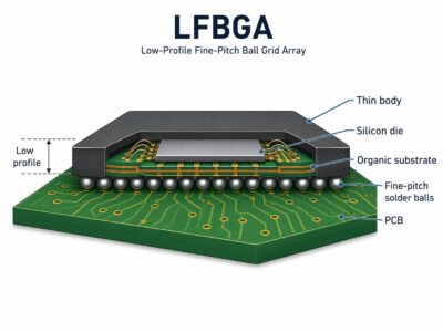
LFBGA means Low-Profile Fine-Pitch Ball Grid Array. The easiest way to think about it is this: it is an FBGA pushed further in the direction of reduced package thickness. The pitch stays fine. The body gets thinner.
That sounds like a small variation, but it matters in products where height above the board is tightly controlled.
LFBGA is used when a design needs all three of these at once:
- relatively high interconnect density
- a compact package footprint
- lower package height
This is especially relevant in devices where the mechanical stack-up is tight—portable products, space-constrained communication modules, handheld industrial units, and compact controller boards. A few tenths of a millimeter in package thickness can matter when the board sits under a display, battery, shield can, or low-clearance housing.
LFBGA does not reduce manufacturing difficulty. It usually increases it.
A thinner package body is often more sensitive to warpage and board-level stress, especially when combined with fine pitch. That means the product gains mechanical packaging freedom while the assembly team gets a narrower process window. PCB routing does not become easier, stencil design still matters, X-ray inspection still matters, and reflow consistency still matters.
LFBGA is a sensible choice for chips that need BGA-level density but are still aimed at compact, height-constrained products rather than extreme-performance computing platforms. Typical examples include:
- compact processors and controllers
- interface devices
- portable communication modules
- consumer and industrial handheld electronics
It is not the most advanced package in the market. It is simply a useful way to keep pushing mainstream BGA packaging toward smaller form factors.
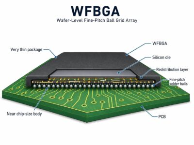
WFBGA is often used to describe a very thin, very small fine-pitch BGA style, sometimes overlapping in practice with wafer-level or near-chip-scale package categories. The naming is not perfectly consistent across suppliers, which is important to acknowledge up front.
What matters more than the label is the design intent: minimal package overhead, very low profile, short interconnect paths, and a footprint that moves closer to the die itself than a conventional laminate-based BGA would.
WFBGA is attractive when the product is so space-constrained that even a normal FBGA starts to look large. That is why this package class is associated with:
- smartphones
- wearables
- TWS products
- compact sensor modules
- PMICs
- RF front-end devices
- highly integrated mobile support chips
The advantage is not just size. Shorter interconnect paths can also help reduce parasitics. But in most real product decisions, the dominant reason is still board space and package height.
WFBGA pushes small-package design far enough that manufacturing tolerance becomes a central issue.
Because the package is so small and thin, board design errors, pad definition mistakes, paste inconsistency, warpage, and alignment variation all become more consequential. Mechanical robustness can also become a concern in environments with board flex, drop shock, or heavy thermal cycling. The package solves a space problem very well, but it does not come with much process forgiveness.
That is why WFBGA is usually a better fit for compact consumer devices than for equipment that prioritizes field repair, heavy mechanical durability, or long-life industrial reliability.
Choosing the right BGA package matters far beyond component selection itself. It directly affects pad design, escape routing, reflow control, X-ray inspection, rework difficulty, and long-term solder joint reliability. In other words, a BGA package that looks acceptable in design can still create assembly problems if the board layout and process window are not matched to it.
For BGA assembly projects, PCBCool supports customers with manufacturing-oriented execution from PCB fabrication through PCBA. Whether the challenge is fine-pitch alignment, warpage control, solder joint consistency, or inspection of hidden joints, our team works to make BGA designs more assembly-ready and more reliable in production.