Printed Circuit Board (PCB) design software is not merely a drafting tool—it is a core engineering system. It governs how schematics are structured, how signals and power are routed, and how reliably a design can move from concept to manufacturing. In real-world engineering environments, choosing the wrong PCB design software often results in layout rework, signal integrity issues, EMI problems, and costly manufacturing delays.
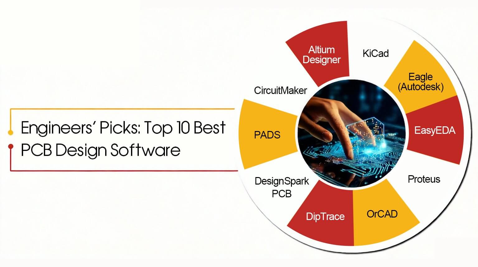
Unlike basic comparison articles, this guide provides an engineering-level evaluation of ten widely used PCB design software tools. Each platform is analyzed based on design philosophy, feature depth, workflow strengths, limitations, and real-world professional use cases. The goal is to help engineers, technical managers, and advanced learners select software based on actual project requirements rather than popularity or marketing claims.
Altium Designer is one of the most widely adopted commercial PCB design software in the industry. It is designed for high-complexity, multilayer, and high-density PCBs commonly used in industrial control systems, consumer electronics, and embedded computing products.
Altium provides a unified design environment where schematics, PCB layout, and component libraries remain fully synchronized. Advanced routing features—such as impedance control, differential pair routing, and integrated manufacturing outputs—are built directly into the workflow.
The software’s greatest strength lies in design consistency and rule-driven control. Engineering change orders (ECOs) are handled automatically, reducing the risk of human error. Its comprehensive rule system helps detect and prevent violations early in the design process, which is critical for dense or high-speed boards. Documentation and fabrication outputs are also mature and production-ready.
However, Altium’s licensing costs are high and generally out of reach for hobbyists or unfunded teams. The software also has a steep learning curve and typically requires a capable workstation to run efficiently.
Overall, Altium Designer is best suited for production-grade PCB development, collaborative team environments, and products approaching mass production.
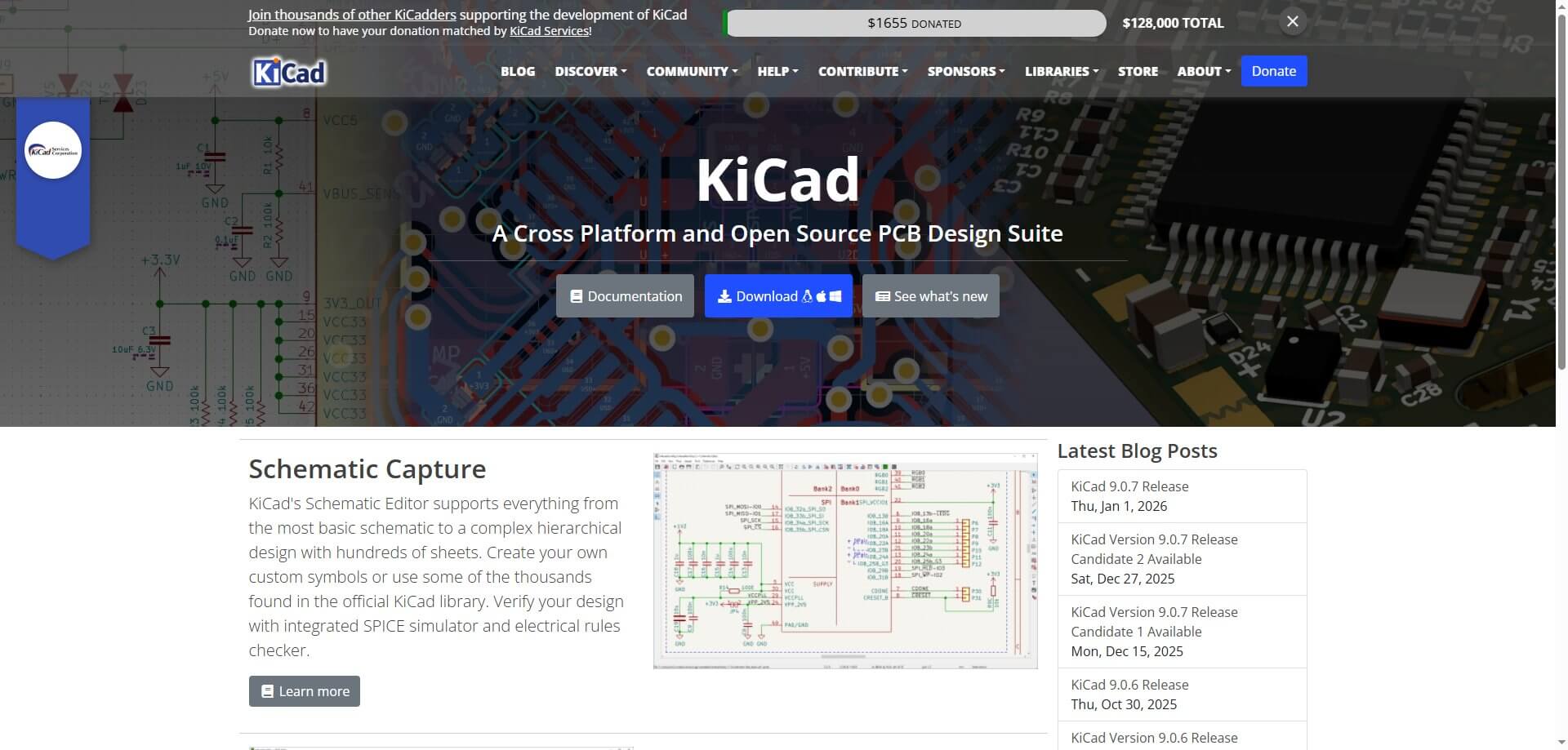
KiCad is a mature open-source PCB design suite that is increasingly used in professional engineering environments. It is commonly adopted by startups, research institutions, and cost-sensitive commercial projects where transparency and long-term accessibility matter.
KiCad supports hierarchical schematics, complex multilayer designs, differential pair routing, and industry-standard Gerber output. Its open file formats ensure that designs remain accessible over the long term without dependency on proprietary licensing or vendor lock-in.
KiCad’s most significant advantage is that it delivers professional-level functionality without licensing costs. Engineers can use the full feature set without restrictions, making it well suited for long-term projects where cost control, auditability, and design ownership are critical considerations.
That said, the user interface is less polished than most commercial tools, and library management requires disciplined processes. Teams without structured library control may encounter symbol or footprint inconsistencies over time.
Overall, KiCad is best suited for professional projects, startups, and engineers who prioritize open ecosystems, cost efficiency, and long-term design independence.
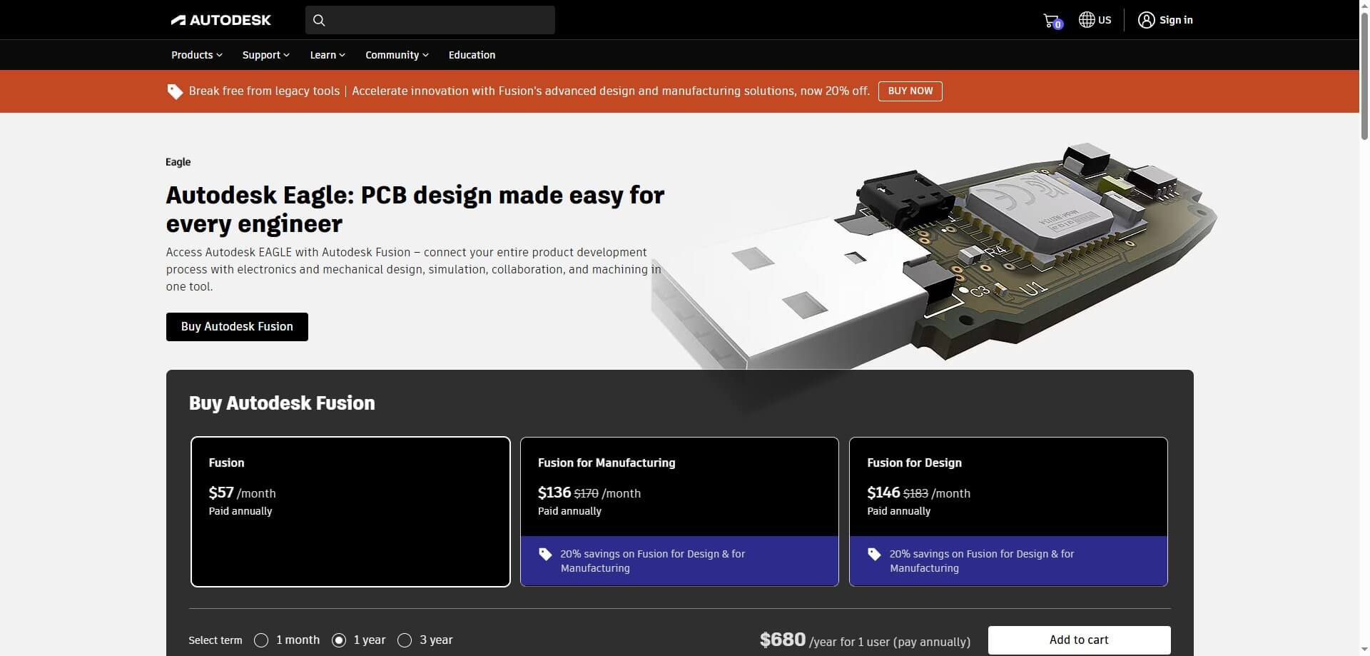
Eagle has long been associated with the Arduino and maker ecosystem and continues to be used for designing small to medium-sized PCBs. Its relatively simple design environment makes it accessible for engineers working on compact boards, early-stage prototypes, and low-complexity hardware projects.
One of Eagle’s core strengths is its straightforward schematic-to-PCB workflow, supported by a large and well-established online component library. The wide availability of open-hardware reference designs in Eagle format further lowers the learning curve and helps accelerate early development cycles.
However, Eagle’s transition to subscription-based licensing, along with board size limitations tied to licensing tiers, reduces its suitability for more advanced projects. Compared with modern professional PCB design tools, its support for high-speed routing, constraint management, and advanced design rules is relatively limited.
EasyEDA is a cloud-based PCB design platform designed to streamline early-stage hardware development by tightly integrating online schematic and PCB layout tools with on-demand manufacturing services. Its web-based environment allows engineers to design PCBs without installing local software, enabling quick access across different systems and locations.
One of EasyEDA’s primary advantages is its high accessibility and fast design-to-fabrication turnaround. Built-in community libraries and direct fabrication ordering significantly reduce the time between design completion and physical prototyping, which is particularly valuable during early validation and proof-of-concept stages.
However, EasyEDA has notable limitations for advanced applications. Compared with desktop professional PCB tools, it offers less comprehensive control over routing, constraint management, and signal integrity. Additionally, its cloud-centric workflow makes it less suitable for confidential designs or highly complex engineering projects.
Overall, EasyEDA is best suited for rapid prototyping, proof-of-concept development, and early design exploration, where speed and convenience outweigh the need for advanced control and fine-grained engineering constraints.
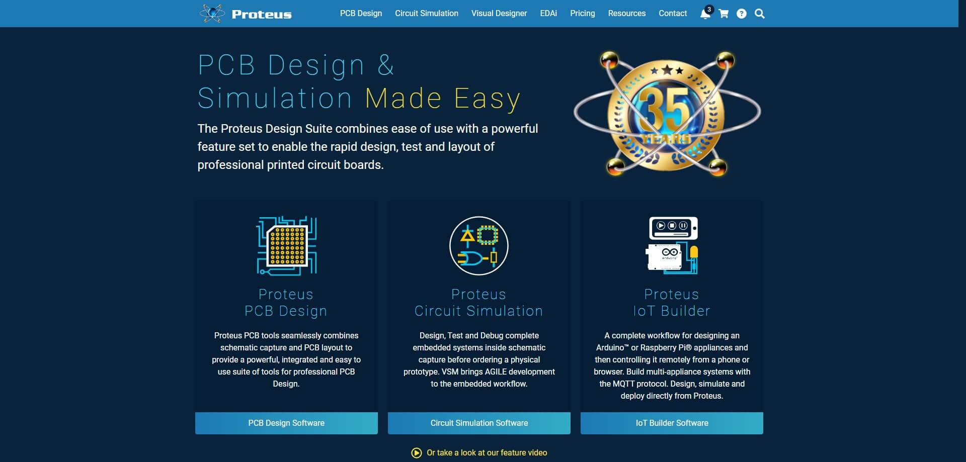
Proteus is a distinct electronic design environment that combines schematic capture, PCB layout, and microcontroller simulation into a single platform. Its defining capability is the ability to run Arduino and other MCU firmware directly on simulated hardware, allowing engineers to evaluate system behavior before investing in physical prototypes.
This simulation-driven workflow is particularly valuable during early development stages, where it helps identify logical errors, incorrect pin assignments, and fundamental timing issues. Early validation of firmware and circuit interaction can significantly reduce the risk of costly hardware revisions later in the development cycle.
However, Proteus is not optimized for final-stage PCB design or manufacturing preparation. Its layout and routing capabilities are less detailed than those of specialized PCB design tools, and its support for advanced constraints and manufacturing-oriented rules is limited. In addition, simulation accuracy depends heavily on the quality and completeness of available component models.
Overall, Proteus is best suited for education, firmware development, and early system-level testing, rather than detailed PCB optimization or production-ready layout work.
OrCAD is a professional PCB design software within the Cadence ecosystem, commonly used in controlled, corporate engineering environments. It is designed to handle large schematics, complex multilayer boards, and projects that must comply with strict electrical and manufacturing requirements.
One of OrCAD’s key strengths is its constraint-driven design methodology. Engineers can define electrical, spacing, impedance, and signal integrity rules early in the design process, ensuring that layout decisions are made in accordance with predefined requirements. This approach significantly reduces late-stage redesigns and engineering corrections.
That said, OrCAD has a steep learning curve. The user interface is complex, and formal training is often required before engineers can work efficiently. Licensing costs are also relatively high, which limits accessibility for small teams and budget-constrained projects.
Overall, OrCAD is best suited for industrial, automotive, and long–life-cycle products, where stability, documentation quality, regulatory compliance, and process control are critical.
DipTrace is a user-friendly PCB design package that delivers professional capabilities without the overhead of enterprise-level tools. It is often chosen by engineers who need more power than entry-level software provides, but do not require the complexity or process rigor of large corporate platforms.
DipTrace offers a clean schematic editor and an intuitive PCB layout environment, with solid routing support for multilayer boards. Its learning curve is significantly gentler than that of Altium or OrCAD, allowing engineers to become productive in a relatively short time.
The platform’s smaller ecosystem is its primary limitation. Compared with more widely adopted tools, DipTrace has fewer commonly used libraries and lower industry penetration, which can slow collaboration in larger or distributed teams.
Overall, DipTrace is well suited for small engineering firms, freelancers, and consultants developing moderately complex commercial PCBs that do not demand advanced enterprise workflows or highly specialized constraints.
DesignSpark PCB is a free PCB design software sponsored by RS Components, designed for engineers who require no license restrictions on board size or layer count. This makes it particularly attractive for cost-sensitive professional projects.
The software provides a stable schematic and PCB layout workflow suitable for standard designs. It supports analog, digital, and mixed-signal boards, provided the designs are not highly complex.
Library management and automation are its main limitations. To ensure precision and maintainability, engineers often need to create and manage their own component libraries.
Overall, DesignSpark PCB is best suited for engineers seeking a free, capable tool who prefer to manage their own designs, especially in projects where cost control is a priority.
PADS is a professional PCB design software with a long-standing use in professional engineering organizations. It bridges the gap between mid-level design tools and full enterprise-grade platforms, offering a balance of capability, control, and production readiness.
The system is valued for its stable layout engine, reliable routing speed, and production-oriented outputs. It supports formal design cycles, making it well suited for team-based environments where process uniformity, documentation, and repeatability are essential. Integration with manufacturing and assembly workflows helps minimize errors during the transition from design to production.
The main limitations of PADS are licensing cost and operational complexity. The software is not entry-level friendly and requires a solid understanding of professional PCB design principles. Formal training is typically needed when onboarding new users.
Overall, PADS is best suited for commercial and industrial design teams where design efficiency, control, and production reliability take precedence over ease of learning.
CircuitMaker is an open-source PCB design software based on the core engine of Altium, targeting the maker and startup community. It provides professional-level schematic and routing tools at no cost.
The main advantage of CircuitMaker is that users can experience Altium-style workflows, including rule-driven design and advanced routing tools. This makes it an effective training platform for engineers transitioning to Altium Designer.
Its primary limitation is that all projects must be open-source, which restricts its use for commercial or confidential projects.
CircuitMaker is best suited for learning, building open hardware, and early-stage experimentation, but it is not intended for closed commercial product development.
In practical engineering, PCB design layout software should be selected based on the project stage and technical complexity, rather than personal preference. During the early stages of development and prototyping, tools like KiCad or EasyEDA are popular among engineers seeking lightweight and versatile platforms. These tools enable rapid schematic and layout development, as well as affordable experimentation without significant licensing costs.
As projects progress toward production, requirements change significantly. Considerations such as manufacturing limitations, documentation accuracy, and implementation of design rules become critical. At this stage, professional-grade tools like Altium Designer or OrCAD are typically adopted, offering robust rule management, strong schematic-to-PCB alignment, and reliable manufacturing outputs.
A common mistake among beginners is choosing PCB software based on popularity or online recommendations. This often leads to frustration when the selected tool does not match the actual project requirements or the user’s skill level.
Another frequent error is rapidly switching between multiple tools. Frequent tool changes prevent designers from developing deep proficiency in workflow, shortcuts, and best practices. Using a single tool consistently improves efficiency, reduces errors, and enhances overall design quality.
Ultimately, the number of tools a designer knows is less important than the ability to master one tool within a structured design process.
PCB design tools have a much greater impact than just board layouts; they determine how efficiently ideas can transform into products. Choosing the appropriate software can minimize design cycles, facilitate brainstorming, and prevent costly production mistakes, while selecting the wrong tool may result in wasted time and repeated redesigns.
Each platform covered in this guide serves a different purpose. Some prioritize flexibility and cost-efficiency, while others focus on advanced rule enforcement, enterprise collaboration, and complex project workflows. Project complexity, compliance requirements, and team experience vary widely, making it impossible to rely on a single tool for all design scenarios.
For engineers and product developers, having a reliable partner for manufacturing and assembly is just as crucial as selecting the right design tool. PCBCool provides complete PCB fabrication and assembly services, helping teams bring their designs to life efficiently, accurately, and at scale. By combining the right software workflow with professional manufacturing support, your ideas can move from schematic to finished product with minimal friction.