After spending time getting a circuit to work on a breadboard, the natural next step is turning it into a reliable, manufacturable printed circuit board. For beginners, this transition can feel overwhelming.
This is where Proteus Design Suite comes in. It provides an integrated environment where you can design schematics, simulate circuit behavior, and develop PCB layouts—all within a single workflow.
In this tutorial, we’ll walk through the complete process of designing a PCB in Proteus. Rather than just showing the steps, we’ll also explain the reasoning behind key decisions along the way.
By the end, you’ll not only have a finished board design, but also a clearer understanding of how to approach your own projects with confidence.
Proteus organizes all design data within a single project. This structure keeps everything consistent and easy to manage from the start, especially as the design becomes more complex.
To create a new project:
- Launch Proteus (IRIS professional).
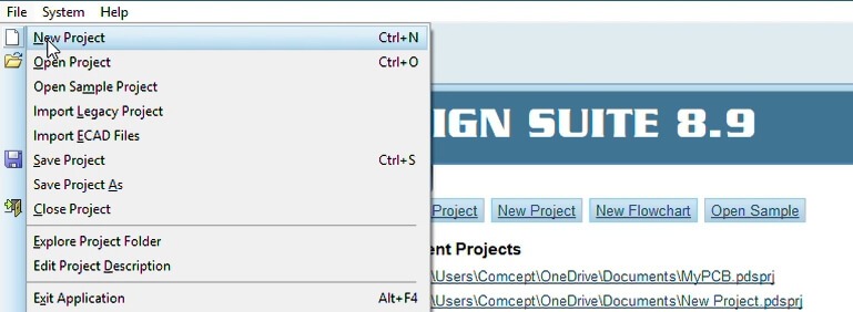
- Go to File → New Project.
- In the project setup dialog, enter a clear and recognizable project name.
- For the template, you can keep the default settings. Make sure the option to create a PCB layout is enabled so the schematic and layout are linked from the beginning.
- Click OK to finish the setup.
Once the project is created, you’ll typically work with two main environments: the schematic capture editor (ISIS) and the PCB layout editor (ARES).
Proteus provides a large built-in library of electronic components, encompassing a wide variety of standard electronic devices. Consequently, in the vast majority of cases, you need only select the required components from this internal library and place them onto your schematic—eliminating the need to import external files.
Each component consists of two parts: a schematic symbol used in the circuit diagram, and a PCB footprint used later during layout. At this stage, we focus on selecting and placing the schematic symbols.
To add components:
- Open the schematic capture editor (ISIS).
- Select Component Mode from the left toolbar (the icon typically shows a resistor).
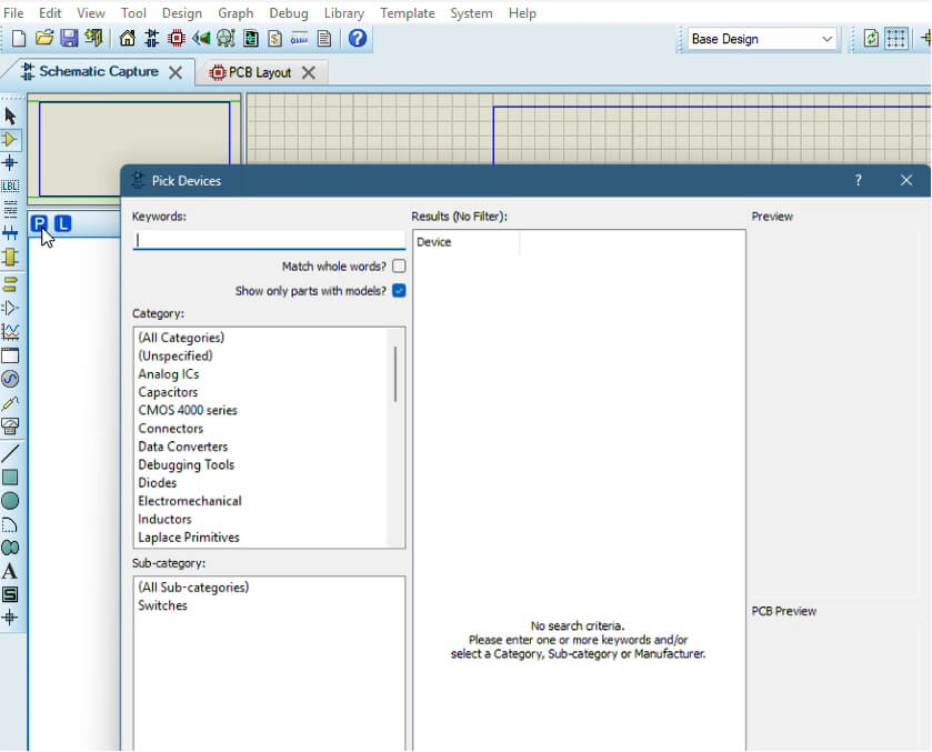
- Click the “P” (Pick Devices) button to open the component library.
- In the library window, search for or browse the components you need.
- Select a component and click OK. It will attach to your cursor.
- Move the cursor to the desired location on the schematic and left-click to place the component.
- Repeat the process until all required components are added to your design.
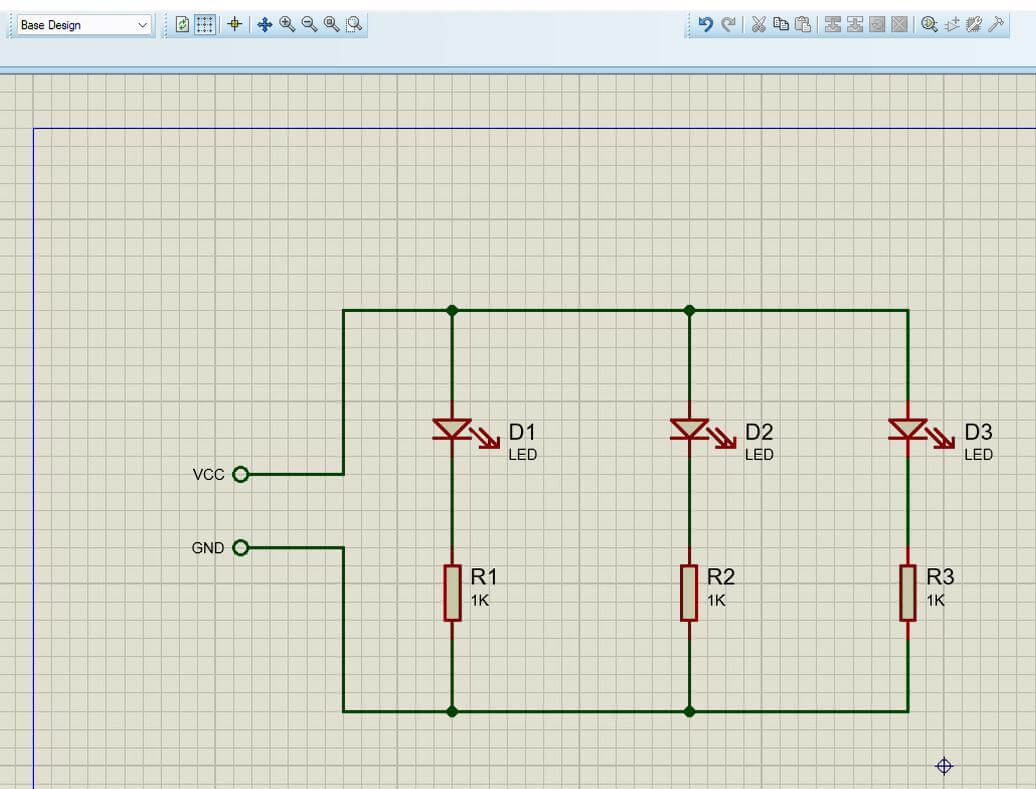
Schematics can be called the universal language of electronics, representing the logical relationships between components rather than their physical placement. Keeping the schematic clear and well-organized at this stage will make the PCB layout much easier later on.
To connect the circuit:
- After placing all components, use the mouse to drag them into a logical layout.
- To draw wires, select the Wire Tool icon from the toolbar.
- Click on a component pin to start a connection, then move the cursor to the target pin and click again to complete the wire. Proteus will automatically create straight or angled connections as needed.
- For power and ground connections, switch to Terminals Mode and place the appropriate power and ground symbols instead of drawing long wires across the schematic.
This is one of the most critical steps in the design process, especially for beginners, as many layout issues originate from incorrect footprint assignments.
A PCB footprint defines the physical dimensions, pad layout, and pin spacing of a component as it will appear on the actual board. In other words, you need to link each schematic symbol to its corresponding real-world package.
To assign or verify footprints in Proteus:
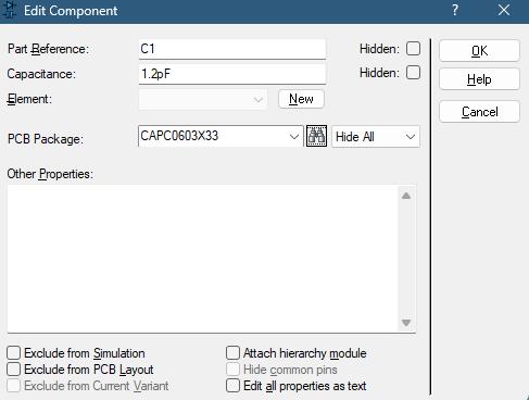
- In the schematic editor (ISIS), right-click on a component and open its Properties (or packaging-related settings, depending on the version).
- Locate the PCB Package field. In some cases, a default footprint may already be assigned, but it should always be verified.
- If you need to change it, click the Add/Remove button next to the package name.
- Choose a footprint that matches the actual component package (for example, DIP, SOIC, or 0603), then confirm your selection.
- Repeat this process for all components before moving on to PCB layout.
Once the schematic is complete and all components have valid footprints assigned, the next step is to transfer the design into the PCB layout environment.
In Proteus, this process generates a netlist—a data structure that defines how all components are electrically connected—and uses it to synchronize the schematic with the PCB layout.
To transfer the design:
- In the schematic capture editor (ISIS), locate the “Update PCB Layout” button in the main toolbar (typically shown as a green arrow).
- Click the button to send the design data to the PCB layout editor (ARES).
- If this is your first time creating the layout, the PCB workspace will open automatically. Otherwise, the existing layout will be updated based on the latest schematic changes.
After this step, all components will appear in the PCB layout area, ready for placement and routing.
A typical two-layer PCB is more like a sandwich, consisting of a top copper layer and a bottom copper layer, separated by an insulating substrate.
The PCB editor uses a layer system to indicate which part of the board you are currently working on.
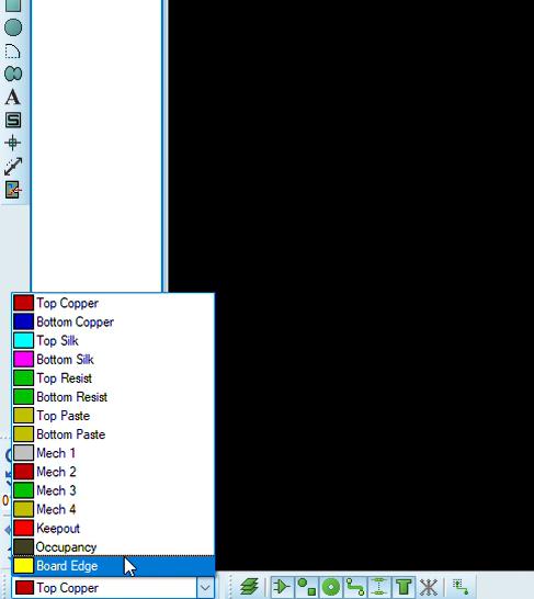
In the PCB layout window, you can find the layer selection controls (usually located in the lower-right area), where each layer is identified by both name and color:
- Top Copper (Red): Used for routing traces on the top side of the board. Surface-mounted components are often placed on this layer, but routing can exist on both sides.
- Bottom Copper (Blue): Used for routing traces on the bottom side of the board. It is commonly used to complete connections that cannot be routed on the top layer alone.
- Top Silk (Yellow): This is the silkscreen layer, used for component outlines, reference designators, and labels printed on the finished PCB.
- Board Edge: Defines the physical outline of the PCB and determines its final shape during manufacturing.
A PCB is not an infinitely extending plane, but rather possesses a specific shape and size. This outline is drawn on the Board Edge layer and will be used by the manufacturer to cut the PCB during fabrication.
To create the board outline:
- Activate the Board Edge layer in the PCB layout editor (usually by selecting its tab in the lower-right corner).
- Select a drawing tool such as the 2D Graphics Box or equivalent tool from the toolbar.
- Click once to start the outline, then drag the cursor to create a rectangle or custom shape.
- Click again to complete the outline
Make sure the board shape is slightly larger than the component placement area to allow for manufacturing tolerances.
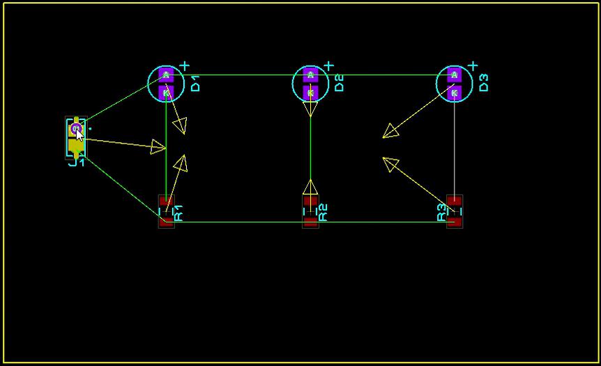
At this step, the PCB design will look like a satisfying puzzle. All you need to do is physically arrange the components so that they align with the circuit’s signal flow logic.
To place components:
- Drag each component into the board outline you created.
- Use the rotation buttons (‘+’ and ‘−’) to adjust orientation for optimal placement.
A practical placement strategy:
- Fixed components first: Place connectors, switches, or mounting holes along the board edges, as their positions are determined by the enclosure or mechanical constraints.
- Critical chips next: Position major ICs, such as microcontrollers, near the center or other strategic locations that minimize trace length.
- Support components nearby: Place resistors, capacitors, crystals, and other passive components close to the pins of the ICs they connect to.
The goal is to minimize trace lengths and avoid unnecessary crossings. Short and direct connections (ratsnest lines) simplify routing and improve signal integrity.
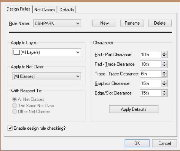
Before routing copper traces, it’s essential to define the design rules for your PCB. These rules specifically define manufacturing constraints, answering questions such as “how much distance should be between two tracks?” or “how thin/thick a track can be?” Correctly setting these parameters ensures your board can be fabricated reliably and helps avoid errors during production.
To set design rules in Proteus:
- Open the Design Rules dialog from the top menu (Design → Set Design Rules).
- Review the available rule categories, including Clearance, Track Width, Hole Size, and others.
- The most critical parameter is Clearance, which defines the minimum distance allowed between copper tracks or pads.
- Click Edit under Clearance and enter a safe value, such as 0.25 mm, which is commonly accepted by many manufacturers.
- Confirm your settings by clicking OK.
Proteus will now monitor your design and flag any violations of the defined rules during routing.
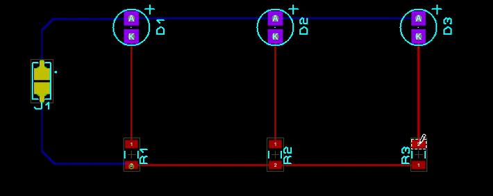
Routing is the process of converting the ratsnest lines into actual copper traces that connect the components. In Proteus, you can route traces manually or use the automatic routing feature. Manual routing is generally recommended, as it gives full control and helps you understand PCB layout principles more thoroughly.
To route traces manually:
- Select Track Mode from the left-hand toolbar (icon resembling a curved track).
- Choose the target layer using the layer selector (for example, Top Copper).
- Click on the starting pad of a component to begin the trace. Move the cursor toward the destination pad, clicking to add corners or change direction as needed.
- Double-click on the destination pad to complete the trace. The corresponding ratsnest line will disappear once the connection is made.
For power and ground connections, it is good practice to use wider traces than for signal lines to ensure sufficient current capacity and reduce voltage drop.
Even after completing your PCB layout, hidden errors can remain. In electronics, a single short circuit or unconnected pin can lead to functional failures. Proteus provides a Design Rule Check (DRC) tool to verify that your board complies with the rules set in Step 9.
To perform a DRC:
- Open the Design Rule Check tool from the menu (Tools → Design Rule Check) and run the check.
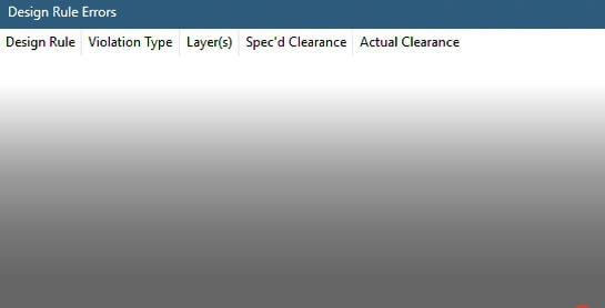
- A report will appear, listing any violations such as Clearance issues or Unrouted Tracks. Proteus will also highlight these errors on the PCB layout.
- Review each issue and correct it before proceeding.
- After the DRC, visually inspect the layout by zooming in to confirm that all traces are properly connected and no pads are left unconnected.
By following the steps outlined in this guide, you have completed a full PCB design cycle using Proteus—from an empty schematic to a verified, ready-to-manufacture board.
While these steps may seem complex at first, they follow a logical progression, and with practice, the process becomes intuitive. Start with simple circuits to build confidence, then gradually tackle more complex designs with multiple components.
Once your design is complete, the next step is turning your concept into a physical board. This is where PCBCool can help. We specialize in manufacturing high-quality PCB from your Proteus designs, ensuring that your ideas are accurately realized in production. Our team can handle everything from prototype boards to full-scale production runs, helping you bring your designs from screen to reality with precision and reliability.