As electronic products get smaller while handling more computing power, packaging technology has had to do more than just hold a chip in place. It now has to support higher pin counts, faster signal transmission, and better thermal performance within a limited footprint.
That is where BGA comes in.
Ball Grid Array, or BGA, has become one of the standard package types used in advanced electronics because it solves several limitations that traditional leaded packages struggle with. Yet many buyers, product managers, and even engineers who are new to electronics manufacturing still think of BGA in very basic terms: a chip with solder balls on the bottom.
That description is not wrong, but it leaves out the part that actually matters. What makes BGA important is not just how it looks, but why its structure works better for high-density, high-performance designs, how different BGA types compare, and what needs close attention during assembly and inspection.
This article focuses on BGA from a manufacturing perspective. Rather than getting lost in theory, it looks at how BGA is used in real production and why it has become a practical requirement in so many modern electronic systems.
BGA stands for Ball Grid Array, a type of integrated circuit package widely used in modern electronics. Components that use this package are often called BGA chips or BGA components.
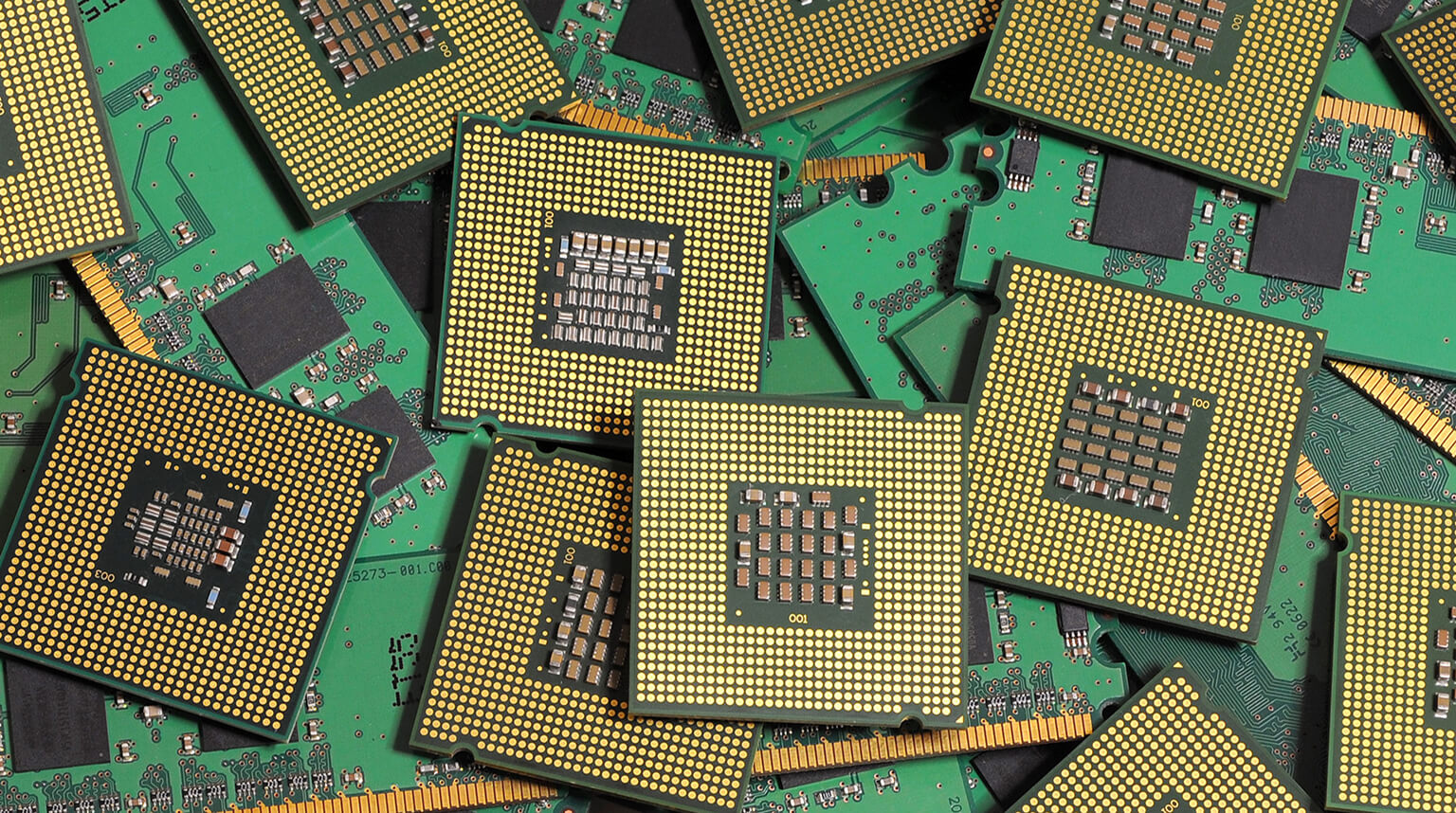
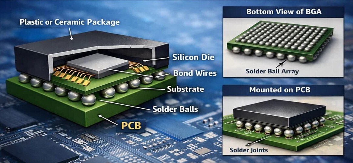
Instead of using leads around the outside of the package, a BGA device uses an array of solder balls arranged across the underside of the component. These solder balls serve two purposes at the same time:
- They form the electrical connection between the chip and the PCB
- They provide mechanical attachment after reflow soldering
A typical BGA package includes three main parts:
- IC die — the functional core of the device
- Package substrate — provides electrical routing and mechanical support
- Solder ball array — connects the package to the PCB
The substrate is usually made from ceramic or organic materials such as BT resin, while the solder balls are typically made from tin-lead or lead-free solder. In many cases, solder ball diameters fall between 0.3 mm and 1.0 mm, and pitch can be smaller than 0.3 mm.
The key difference from traditional packages is structural. Conventional leaded packages place interconnections around the perimeter. BGA uses the entire bottom surface. That shift is what gives BGA its main advantage: more connections in less space, with better electrical and mechanical behavior.
The biggest difference between BGA and traditional leaded packages is where the connections are placed.
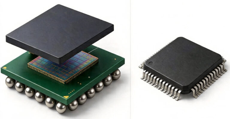
In packages such as QFP, leads have to be routed around the outer edges of the body. That means available interconnect area is limited to the perimeter. As I/O count rises, designers usually face two choices: make the package larger or reduce lead pitch to the point where manufacturing becomes more difficult and yield becomes harder to control.
BGA changes that constraint by moving the connections underneath the package in a grid pattern. Instead of relying only on the outer edge, it turns the full bottom surface into usable interconnect area.
That is why BGA is commonly used for processors, GPUs, memory devices, and other components that may require hundreds or even thousands of connections.
In a conventional leaded package, the signal typically travels from the die through the internal package connection and then through relatively long external leads before reaching the PCB. Those longer conductive paths add parasitic inductance and resistance. At higher speeds, those parasitics start to matter more because they can distort signals, increase noise sensitivity, and make signal integrity harder to control.
With BGA, the interconnections are formed through solder balls directly beneath the package. That creates a shorter, more direct path from the device into the board.
The improvement is not just theoretical. A shorter interconnect path generally means lower parasitic effects, which makes high-speed signals easier to manage and reduces the margin for signal degradation.
As device performance increases, power density usually rises with it. More heat is generated in a smaller area. If that heat cannot move out of the package efficiently, junction temperature increases, and that can affect performance, long-term reliability, and product life.
In many traditional leaded packages, because much of the package structure and connection scheme is concentrated around the perimeter, heat often has to travel through less efficient routes before it can be spread through the PCB.
BGA improves this because the solder ball array sits directly underneath the package. That bottom-side interconnect structure creates a more direct transfer path from the package into the board. Once heat enters the PCB, it can be distributed through copper planes, thermal vias, and other board-level thermal design features.
Traditional leaded packages also have a mechanical weakness: the leads are exposed.
During shipping, storage, handling, placement, or rework, those leads can be bent or deformed. Once that happens, the component may not sit flat on the board, which can lead to coplanarity problems, poor solder joints, or placement failure.
BGA avoids that issue because it does not depend on exposed perimeter leads. The interconnects are protected underneath the package body, making the device less vulnerable to mechanical damage before assembly.
BGA also benefits from a self-alignment effect during reflow. When the solder balls melt, surface tension naturally helps pull the package into alignment with the PCB pad pattern.
PBGA is the most common general-purpose BGA type.
It typically uses a plastic substrate, often based on BT resin or glass laminate. Because the process is mature and relatively cost-effective, PBGA has become the most widely used BGA category in the market. Its solder ball diameter is usually in the 0.75 mm to 1.0 mm range, with pitch commonly around 1.27 mm.
That combination makes PBGA a practical choice for medium- to high-density applications where cost control is still important.
CBGA uses a multilayer ceramic substrate and is typically sealed with a metal lid for hermetic packaging.
Compared with plastic-based packages, ceramic construction offers better resistance to high temperature, radiation, and moisture. That makes CBGA more suitable for harsh environments and applications with demanding reliability requirements. Its solder balls usually use high-melting-point alloys, which further support thermal stability.
The tradeoff is cost. CBGA offers stronger environmental performance, but at a significantly higher price point than standard PBGA.
FCBGA combines BGA packaging with flip-chip die attachment.
In this structure, the active side of the die faces downward and connects directly to the substrate through solder bumps rather than traditional wire bonding. That further shortens the electrical path, reduces parasitic inductance, and supports higher overall performance.
FCBGA can also support very fine pitch, sometimes below 0.3 mm, which makes it well suited for devices that need extremely high interconnect density.
There are also other BGA variants designed for more specific use cases. Examples include:
- FBGA (Fine-Pitch Ball Grid Array) for compact devices
- EBGA (Enhanced BGA) for higher-power applications
In practice, the right BGA type depends less on the acronym itself and more on the design priorities behind the product: size, power, performance, environment, and cost.
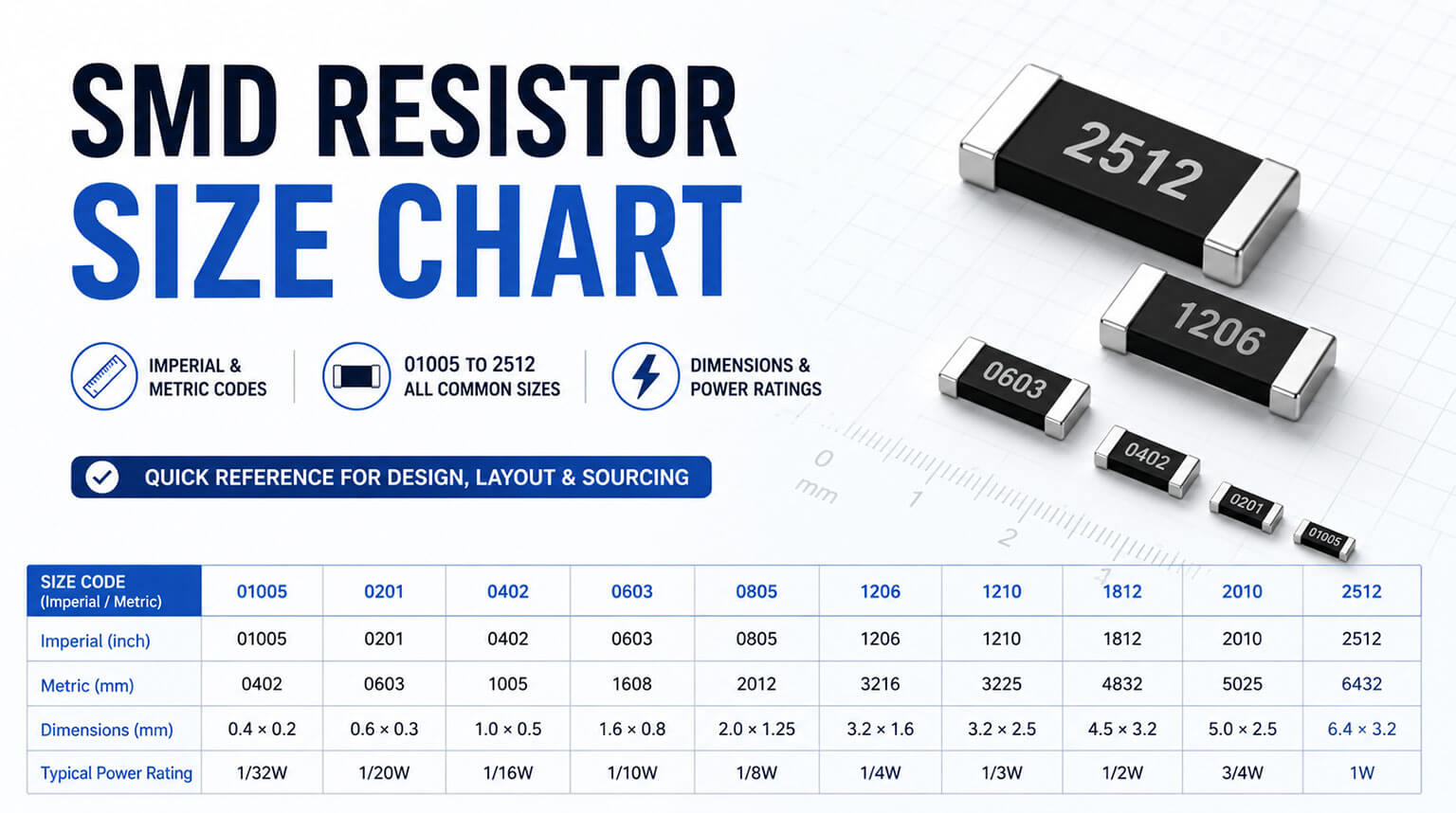
Like other SMD components, BGA devices are assembled on automated SMT lines through solder paste printing, component placement, and reflow soldering.
The difference is that BGA packages require tighter placement control because the interconnects are underneath the body rather than visible around the edges. As pitch gets finer, the tolerance for placement error gets smaller. That can slow overall throughput, especially in projects with dense boards or aggressive turnaround targets.
Manufacturers often address this by configuring SMT lines with multiple placement machines so components with different complexity levels can be distributed more efficiently across the line.
Inspection is one of the biggest practical challenges in BGA assembly.
With leaded packages, many soldering issues can be identified visually or through AOI. With BGA, the critical joints are hidden beneath the package body, so standard optical inspection can only verify what is visible on the outside. It cannot directly confirm the internal condition of the solder joints.
That is why BGA projects typically require more than AOI alone. X-ray inspection is commonly used because it allows the assembler to examine hidden joints under the package and identify issues such as voids, cold joints, missing balls, or bridging that would otherwise go undetected until field failure.
This happens when the solder balls do not fully fuse with the PCB pads, resulting in weak electrical or mechanical connection.
Typical causes include insufficient solder paste, an inadequate reflow profile, or oxidation on the pads. In practice, this is not just a process problem at one step. It is often the result of several small issues stacking together: uneven paste deposition, incomplete wetting, and insufficient thermal energy during reflow.
Common corrective actions include:
- Optimizing solder paste printing to ensure stable paste volume on each pad
- Adjusting the reflow profile, including soak time, to improve wetting behavior
- Cleaning or otherwise preparing pads to reduce oxidation before assembly
Bridging occurs when adjacent solder balls connect during reflow and create a short circuit.
This is often related to overly tight pitch, excessive solder volume, or placement offset. In other words, it usually comes from the interaction between design tolerance and process control, not from one isolated mistake.
Solutions typically include:
- Optimizing PCB pad design
- Controlling solder paste volume more carefully
- Calibrating placement accuracy to reduce offset during mounting
Package cracking is seen more often in PBGA packages.
The main causes usually include poor moisture control before reflow, overly aggressive temperature ramp-up, or mechanical stress during handling and placement. Moisture is especially important because absorbed moisture can expand rapidly during heating and damage the package structure.
Typical prevention methods include:
- Following moisture control and baking procedures carefully
- Optimizing the reflow heating rate
- Reducing squeezing or mechanical stress during placement and handling
BGA matters not because it is considered high-end, but because it solves specific problems that older package types cannot solve well once a design reaches a certain level of complexity.
When a product requires higher interconnect density, better signal behavior, and more effective thermal transfer into the PCB, BGA often becomes the practical choice rather than an optional upgrade. At the same time, not every design needs it. For simpler products, a traditional package may still be more economical and easier to manufacture.
At PCBCool, we support BGA projects through one-stop service, from bare PCB manufacturing that protects pad quality, to sourcing hard-to-find BGA components, to BGA assembly with pitches as fine as 0.25 mm.