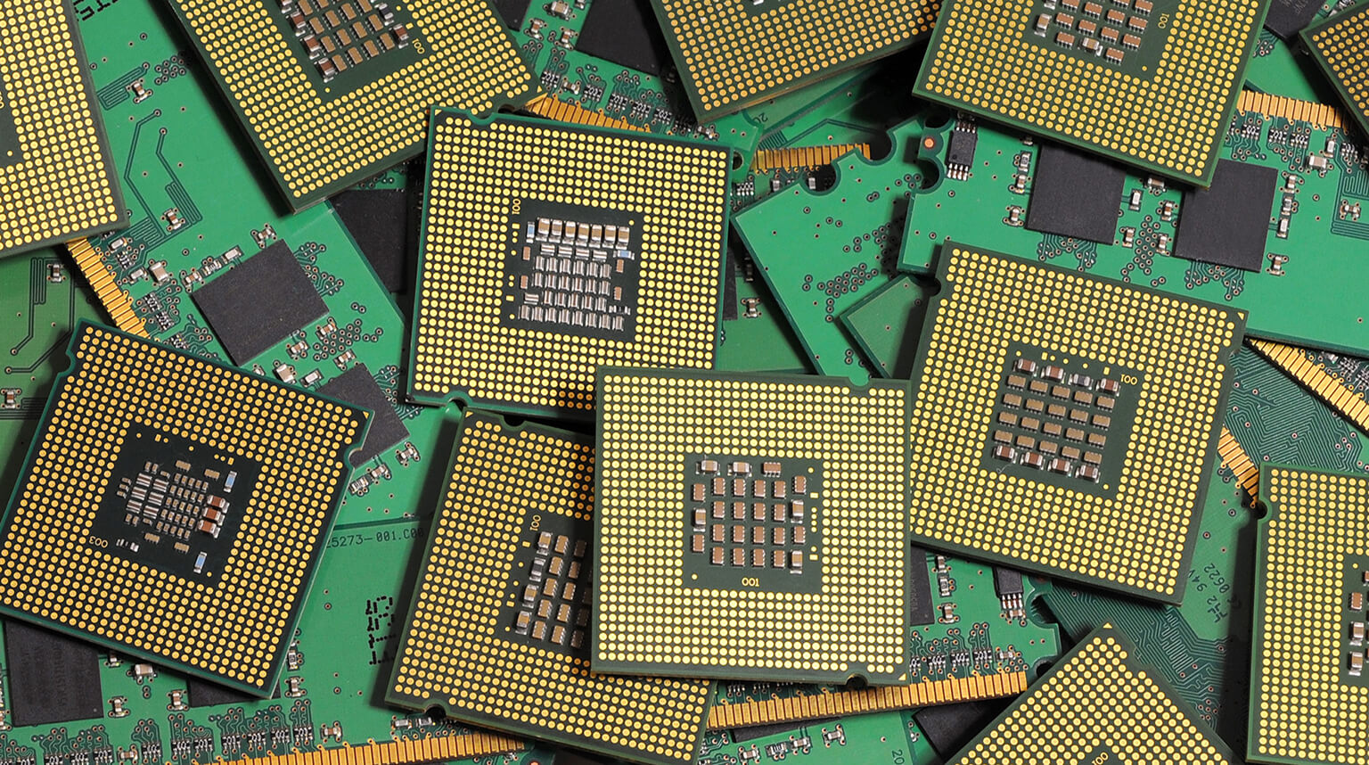
BGA (Ball Grid Array) packages sit at the heart of almost every modern board worth talking about — the application processor in a smartphone, the FPGA in an industrial controller, the GPU on a graphics card, the SoC on a single-board computer. Their dense pin layout and short signal paths make them ideal for high-speed, space-constrained designs.
But that same density is exactly why BGA chips are so painful to repair. There are no exposed leads to probe, no individual pins to reheat one at a time. Every solder ball sits hidden underneath the package, and when one fails, the whole component effectively has to come off and go back on as a unit.
This article covers why BGA chips fail in the first place, what the rework process really involves step by step, how to judge whether a repair is worth attempting at all, and what you can do at the design and assembly stage to avoid ending up here.
BGA failures are rarely about the silicon itself. In the overwhelming majority of cases the chip is fine; it is the solder joints connecting it to the board that have given out. A few mechanisms account for most of what you will see on a bench:
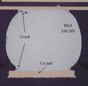
This is the primary cause of BGA chip failure, as the package and the underlying PCB are made of different materials, so they expand and contract at different rates as temperature changes. This difference is described by the coefficient of thermal expansion (CTE).
During normal operation, repeated power cycling, or use in hot environments such as sealed enclosures exposed to sunlight, the package and PCB move slightly against each other. The solder balls absorb this movement as mechanical stress.
After many thermal cycles, microscopic cracks often begin at the outer corner solder balls, where shear stress is highest. As cycling continues, these cracks can gradually propagate toward the center of the array. This is why a device may operate normally for months or even years, then begin to show intermittent faults before complete failure occurs. The cracks were growing the whole time.
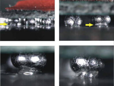
BGA chips are mounted onto circuit boards using SMT and soldered reflow; process defects can easily lead to the “head-in-pillow” and voiding defects.
Head-in-pillow defects happen when the solder ball and the solder paste on the pad both melt during reflow but never fully merge into one continuous joint, usually because of an uneven reflow profile or a warped package.
Voiding refers to gas pockets trapped inside the solder ball during reflow; these reduce the cross-sectional area carrying current and heat, making that joint the first to fail under stress.
Neither of these is visible from outside the package; they only show up under X-ray or once the board is already misbehaving in the field.
Sometimes called the “popcorn effect,” is specific to plastic-packaged BGAs. These packages are hygroscopic; they absorb a small amount of moisture from the air over time.
If a moisture-saturated package is then reflowed (during the original assembly or during a rework attempt) without first being baked dry, that trapped moisture flashes to steam inside the package and can delaminate the internal layers or even crack the package body.
This is exactly why moisture sensitivity level (MSL) ratings and bake-before-reflow procedures exist, and skipping them is a common cause of “it worked until we touched it” failures.
Board flex during installation, vibration in field-deployed equipment, drop shock, or poor support during transport can all place stress on the solder ball array.
Flux residue left under a package after assembly can also slowly corrode pads over months, especially in humid environments, something worth keeping in mind for any board destined for outdoor or industrial use.
Desoldering and reinstalling BGA components is a risky undertaking; regardless of your technical proficiency, it is best to diagnose the component and confirm it is indeed the source of the problem before attempting a rework.
Boundary-scan or JTAG testing, continuity checks on accessible signals, and thermal imaging under load can all point to a suspect device.
X-ray inspection is the most useful single step here — it lets you see the ball array underneath the package and spot cracked, bridged, or voided joints without removing anything.
If the board has been stored in an uncontrolled environment, or if the package has an MSL rating that’s been exceeded, bake it at a low temperature (commonly 100–125°C for several hours, depending on package thickness and MSL level) before any reflow step.
This isn’t optional theater; it is what prevents the popcorn cracking described above.
This process is similar to baking but serves a different purpose; it does two things: reduces the thermal gradient the board experiences during the actual removal (which is what causes warping); shortens the time the hot air tool needs to spend on the top side, reducing the risk of damaging neighboring components.
It is important to note that this process applies to the entire assembly rather than just the chip; the whole board is brought up to an intermediate temperature, typically 100–150°C, using a bottom-side preheater or hot plate.
With the board preheated, a hot air rework station directs heated air specifically over the target BGA until the solder reaches its liquidus point, around 183°C for leaded (Sn63/Pb37) solder, or roughly 217–220°C for lead-free SAC alloys.
Once the balls are molten, the component can be lifted using a vacuum tweezer. Timing is really important: lifting too early shears partially molten joints and risks damaging the package or the pads; lifting too late starts cooking neighboring components unnecessarily.
Once the chip is off, the old solder needs to come off the pads completely and evenly. Leftover solder mounds will throw off the alignment of the new component and cause uneven joints later.
This is usually done with solder wick and a soldering iron, or with hot air and a solder vacuum, followed by flux residue cleanup with isopropyl alcohol.
At this stage, it is also worth inspecting the pads under magnification for lifted or damaged pads. A lifted pad is often the point where a “simple” rework turns into a board-level repair.
If you are reusing the original chip, fresh solder balls need to be applied in place of whatever was left after removal. Old balls are rarely uniform enough to reflow cleanly a second time.
A reballing stencil matched to the package’s ball pitch sits over the chip, solder paste or preformed balls are applied through it, and the assembly goes through a controlled reflow to form new balls.
If you are installing a brand-new replacement chip, this step can be skipped since the chip is usually pre-balled; simply apply solder paste to the circuit board pads.
This is the step where precision matters most, and it’s also the step most prone to silent failure. Since BGA pitches can be as fine as 0.4 mm, an offset of even one-quarter of a solder-ball diameter may cause solder bridging between adjacent pads.
To prevent this, the rework station’s split-vision or optical alignment system aligns the chip’s ball pattern with the PCB pad pattern before placement. Once the component contacts the solder paste, it can no longer be reliably adjusted.
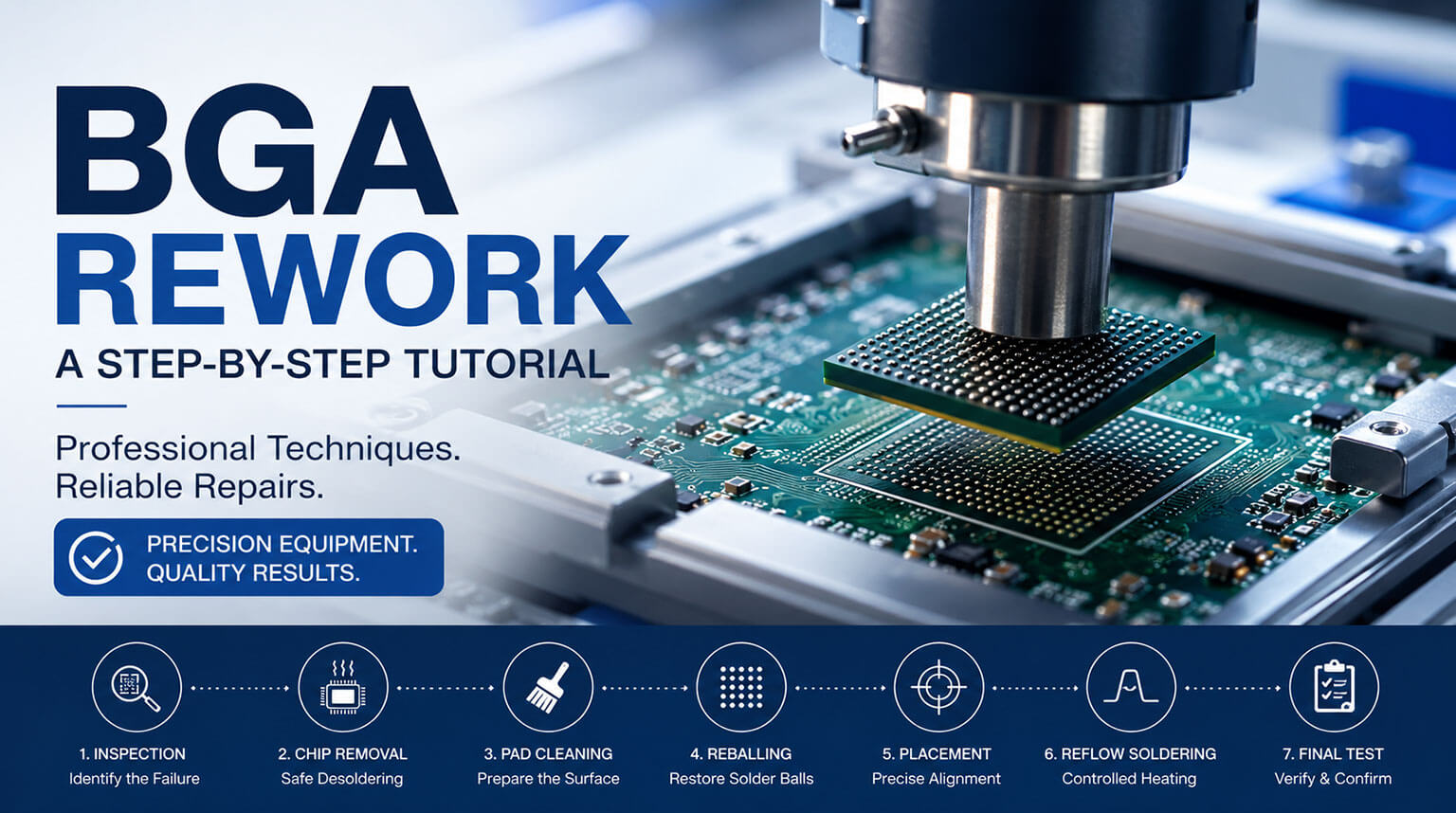
This is the heart of the whole process, which typically includes the following four stages:
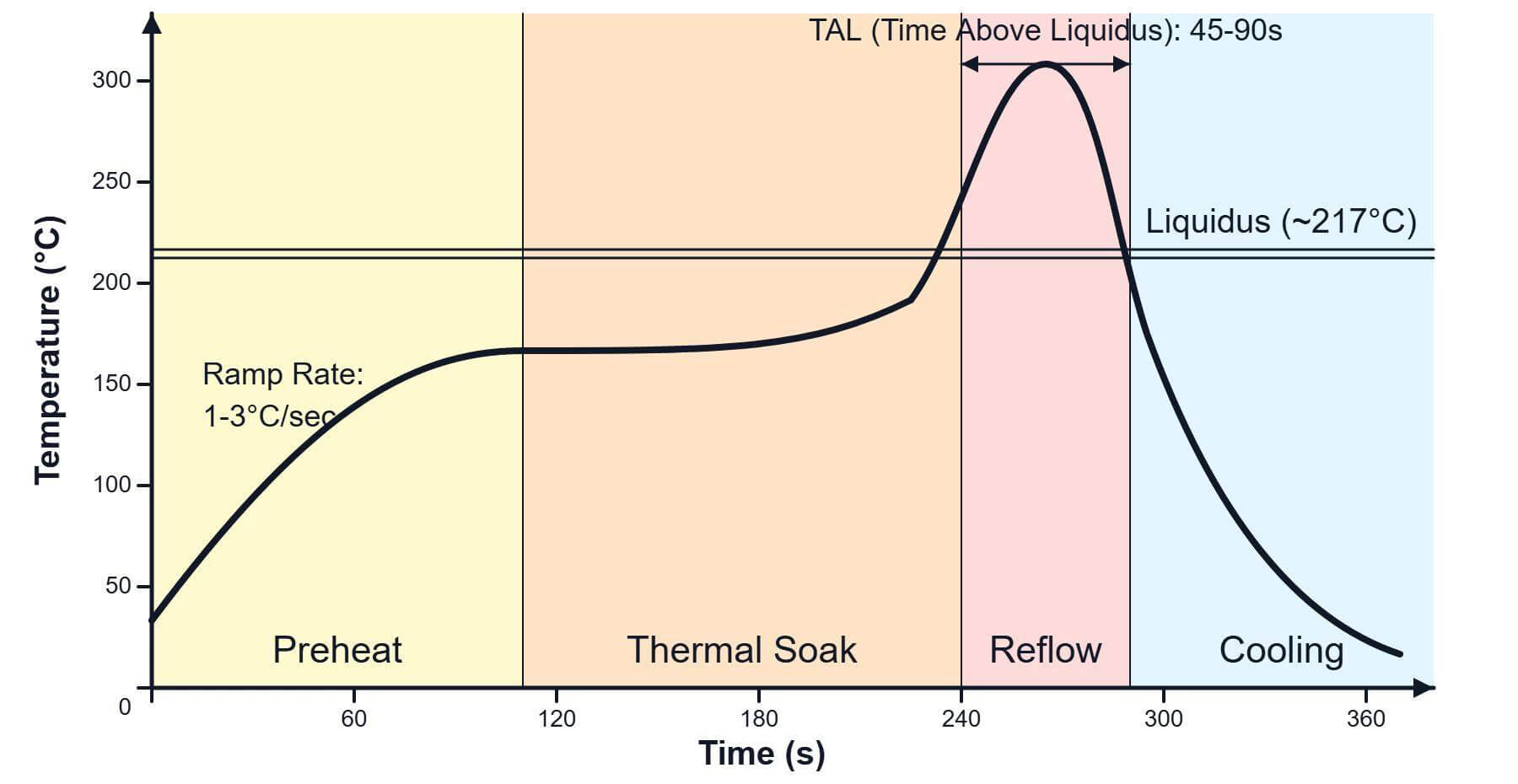
- Gradual preheat ramp (typically 1–3°C per second) up to a soak temperature around 150–180°C held for 60–120 seconds to let the whole assembly reach thermal equilibrium and activate the flux;
- Ramp to peak reflow temperature, usually 20–30°C above the solder’s liquidus point (so around 235–245°C for lead-free);
- Brief time-above-liquidus window of roughly 30–60 seconds to let the joints form properly without overheating the package;
- Controlled cooling ramp back down, ideally no faster than 3–4°C per second, to avoid thermal shock that can crack a freshly-formed joint or warp the board.
X-ray inspection again, this time to confirm there’s no bridging, no excessive voiding, and that the ball array looks uniform. A continuity and power-on functional test follows.
However, A board that powers on but hasn’t been checked under load or stress can still be hiding a marginal joint that fails again in a week.
Not every BGA failure deserves a rework attempt, and knowing when to stop is as much a part of the job as knowing how to solder.
If the failed chip is a low-cost, widely available part, replacing the whole board or module can be cheaper and lower-risk than rework once labor time is factored in. The calculation flips for expensive or obsolete parts, a legacy FPGA or an end-of-life processor that’s no longer manufactured may make rework the only realistic option, regardless of labor cost, because there’s no replacement board to buy.
Board complexity and layer count matter more than people expect. The more complex the board, the higher the risk that “fixing” one component creates a second problem somewhere else. A simple two- or four-layer board tolerates rework heat reasonably well. A high-layer-count board with buried vias, fine-pitch routing near the BGA, or other heat-sensitive components nearby is much more likely to suffer collateral damage — warping, delamination, or damage to adjacent parts — during the preheat and reflow cycle.
Reworking history is worth checking before starting. Each reflow cycle a board goes through degrades the PCB material slightly. As pad adhesion weakens, the solder mask becomes more brittle, and the risk of lifted pads or trace damage increases. A board that’s already been reworked once or twice has a meaningfully lower chance of surviving another cycle cleanly, and that should factor into the decision.
For a one-off prototype or a single field unit, rework is usually the right call. It is faster and cheaper than redesigning anything. If the same failure is showing up across many units of a production run, the more valuable fix is root-cause analysis. Was it a reflow profile issue at the contract manufacturer, a design issue with insufficient thermal relief, or a batch of bad components? Confirming this is better, rather than reworking each unit individually. Reworking symptoms while ignoring a systemic cause just guarantees you will be doing this again.
Design for thermal and mechanical reliability from the start. Proper land pattern design, adequate thermal relief on ground and power pads, and via-in-pad techniques for fine-pitch parts all reduce the stress concentration at corner balls. Where the application involves significant vibration or repeated thermal cycling — outdoor enclosures, automotive, industrial equipment — adding underfill epoxy beneath the BGA after assembly mechanically reinforces the solder joints and dramatically improves fatigue life, at the cost of making future rework essentially impossible. That trade-off is worth making consciously rather than by default.
Store moisture-sensitive components in sealed, desiccant-protected packaging, track floor life once a package is opened, and bake parts that have exceeded their MSL exposure window before they go through reflow. This single procedural step prevents a large share of the “intermittent failure that started after a repair” cases.
Control the manufacturing reflow profile, not just the rework profile. A poorly controlled profile at the original assembly stage — too fast a ramp, an inadequate soak, an uneven preheat across the board — bakes voiding and head-in-pillow defects into joints before the product ever ships. Automated optical inspection and X-ray sampling during production catch these defects before they reach the field, where they’re far more expensive to deal with.
Conformal coating protects against humidity and contamination in harsh environments; proper enclosure design and mounting reduce mechanical stress and vibration transmitted to the board; and adequate thermal management — heatsinking, airflow, or simply not running a chip near its thermal limits continuously — slows the rate of thermal cycling fatigue over the product’s lifetime.
BGA rework is a high-risk process. Any mistake during removal, cleaning, alignment, reflow, or inspection can cause permanent damage to the component or the PCB. In many cases, the most cost-effective BGA rework is the one that never has to happen — because the risk has already been reduced through proper design review, controlled assembly, and reliable inspection.
If your PCBA project involves BGA components, PCBCool’s BGA assembly service can help reduce that risk from the start. We use Panasonic NPM-W2 pick-and-place equipment and a JTR-1000D reflow oven to support accurate BGA placement and controlled soldering. X-ray inspection is also integrated into our BGA assembly workflow to check hidden solder joints, detect bridging or voiding, and improve overall assembly reliability.