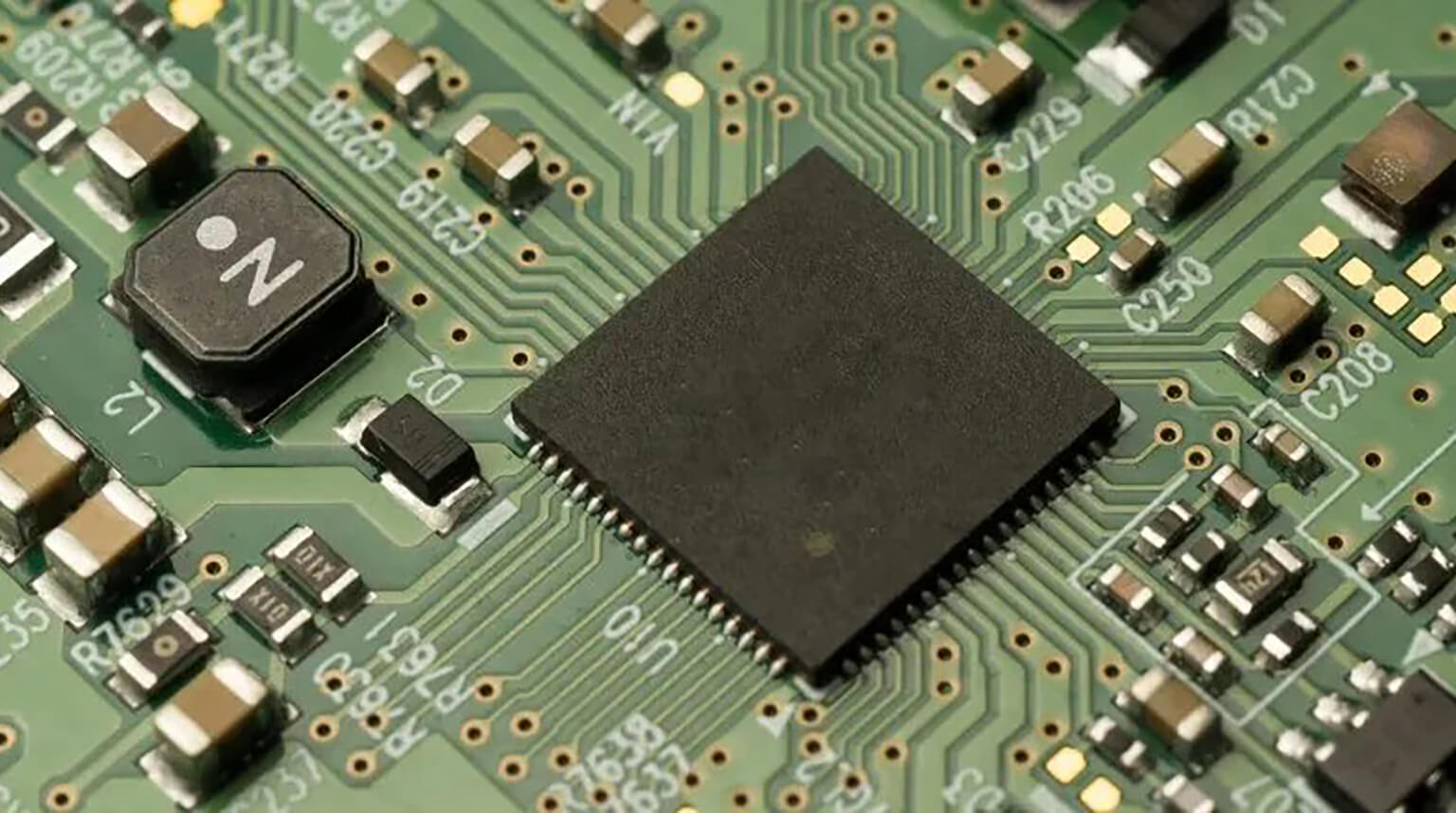
In modern electronic products, devices are becoming smaller, more powerful, and faster. At the same time, PCB routing density continues to rise: more components, denser BGAs, and more complex high-speed signal paths. For many high-end applications, traditional multilayer PCB structures are no longer the most efficient solution.
To address these bottlenecks, HDI (High-Density Interconnect) PCBs have emerged. The core idea of HDI is to achieve higher routing density and better electrical performance in limited space by using smaller trace widths and spacing, smaller microvias/blind vias, and tighter interlayer connections.
Among the various HDI structures, 1+N+1 is one of the most common and also one of the easiest for engineers to master. It organizes the PCB as a top layer + multi-layer core + bottom layer, and uses sequential lamination to reliably manufacture microvias and buried vias.
If you’re not familiar with it yet, let’s start learning about it now.
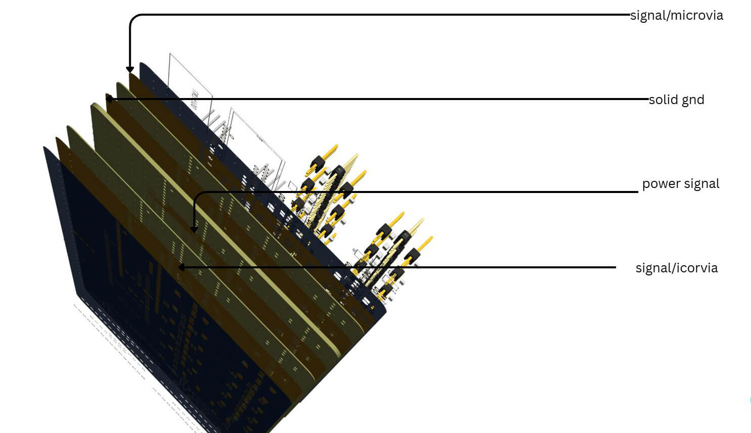
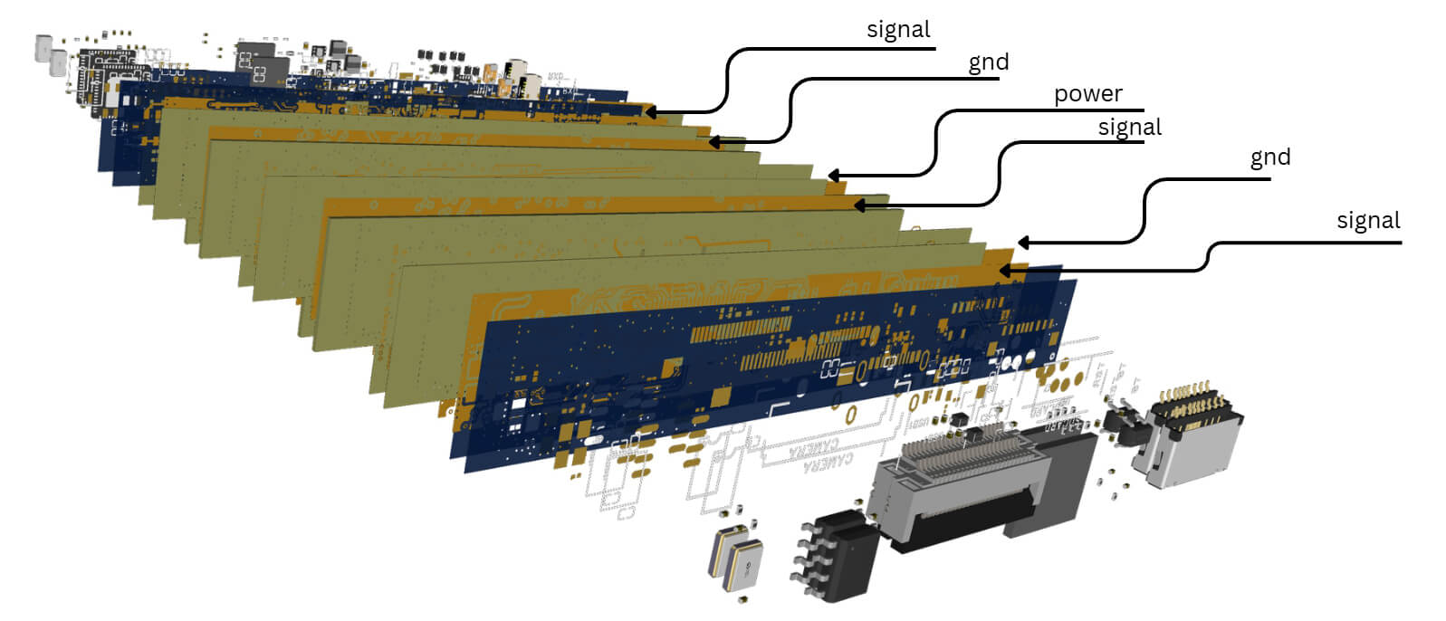
The notation 1 + N + 1 is one of the most common (and most frequently misinterpreted) ways to describe an HDI build-up stackup. It refers to the build-up structure and manufacturing sequence, not just the final number of copper layers.
- 1 = One build-up layer (sequential lamination + microvias) on the top side
- N = The central core (usually a conventional multilayer section with through-holes or buried vias; in many practical cases it has an even number of layers for symmetry, but this is not mandatory)
- 1 = One build-up layer (sequential lamination + microvias) on the bottom side
Typical stackups include the 1+2+1 and the 1+4+1:
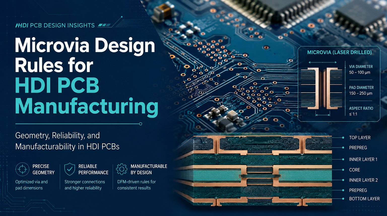
The outer “+1” layers support laser-drilled microvias (typically 0.08–0.15 mm diameter) that connect the outer layers to the next inner layer or the core, depending on the design. These small vias free up surface space for dense BGA fanout and fine-pitch routing, which is extremely difficult with standard through-hole vias in conventional multilayer boards.
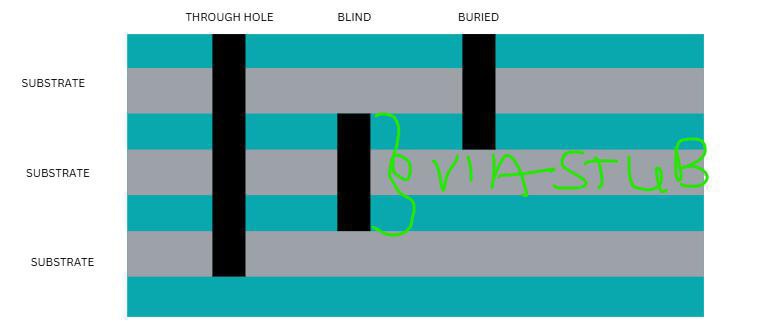
Microvias are much shorter than through-hole vias, dramatically reducing via stub length and the associated parasitic inductance/capacitance. This is especially beneficial for high-speed signals (PCIe, USB 3.x, DDR4/5, MIPI, etc.), where long stubs can cause severe reflections and signal degradation.
Because microvias reduce the need for long through-holes and allow more flexible layer stacking, 1 + N + 1 boards can be thinner than equivalent-density conventional multilayers. This is critical for smartphones, wearables, tablets, and other space-constrained devices.
| Aspect | Standard Multilayer PCB | HDI with 1+N+1 Structure |
|---|
| Lamination process | Typically a single lamination cycle | Sequential lamination (at least 2 cycles) |
| Via types | Mainly through-hole vias | Microvias (laser) + through-hole vias (blind vias may be used depending on design) |
| Via size | Typically ≥ 0.2–0.3 mm, depending on fab capability | Microvias ~0.08–0.15 mm |
| Line/space capability | 4/4–5/5 mil typical | 3/3 mil or finer on outer layers |
| Outer layer density | Normal | High (for fine-pitch BGAs, dense routing) |
| Cost | Lower | Higher (but can reduce total layers needed) |
In 1 + N + 1 HDI PCBs, vias are the unsung heroes that enable dense routing, signal integrity, and compact form factors. Without advanced via technology, you’d be stuck with bulky through-holes eating up valuable space.
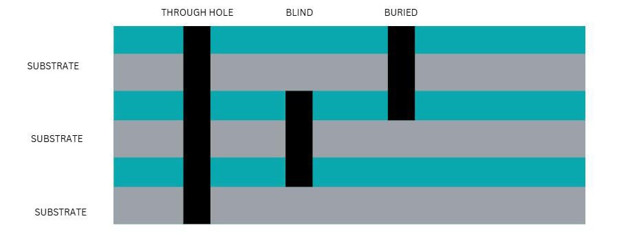
Microvias are small, shallow vias (typically 0.08–0.15 mm diameter) that connect only adjacent layers in the build-up sections. They’re what differentiate HDI from standard multilayers.
Unlike mechanical drilling, microvias are created using CO₂ or UV lasers for precision and minimal damage. This enables precise hole formation in thin dielectrics and is essential for fine-pitch designs.
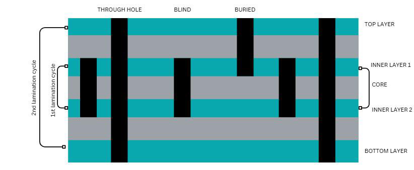
These vias are fully internal to the core (N layers), connecting inner layers without reaching the outer surfaces (e.g., L3 → L4 in a 1+4+1 stackup). They’re drilled and plated before the outer build-ups are added. Buried vias improve inner-layer routing density but cannot be used for surface connections—they’re “buried” during final lamination. They are often used for power distribution or signal transitions in the core without cluttering the outer layers.
The classic via type: drilled through the entire board (L1 to L(N+2)) and plated for conductivity. In 1 + N + 1, they’re used sparingly for global connections like power/ground stitching or where microvias aren’t sufficient. They’re larger (typically ≥ 0.2–0.3 mm) and can create stubs in high-speed designs, so backdrilling is often required for critical signals. However, they remain reliable and cost-effective for non-critical paths.
Sequential lamination is a manufacturing process where a PCB is built in stages, rather than all at once.
Instead of pressing all copper layers together in a single lamination cycle, the process is split into multiple steps:
- The core (N layers) is laminated first
- Additional build-up layers are added one at a time on each side
- After each build-up, microvias are drilled and plated, and then the next lamination cycle begins
This staged approach enables the creation of microvias and reliable HDI structures.
In conventional multilayers, through-hole vias create long unused stubs that introduce impedance discontinuities and reflections, leading to ringing and eye closure at high speeds. Sequential lamination enables blind microvias that stop exactly where needed (e.g., L1 to L2 only), eliminating or drastically shortening stubs.
Laser-drilled microvias have smaller barrels and higher drilling precision, resulting in more controlled impedance transitions when signals move between layers.
Shorter vias and thinner overall board thickness can reduce dielectric and conductor losses at high frequencies. Sequential build-up also lets you choose dielectric materials per section, enabling better optimization for minimal attenuation.
The biggest rookie (and not-so-rookie) mistake is assuming microvias behave exactly like through-hole vias.
Microvias are blind, short, and limited to adjacent layers — you can’t route a signal through four layers using a single microvia.
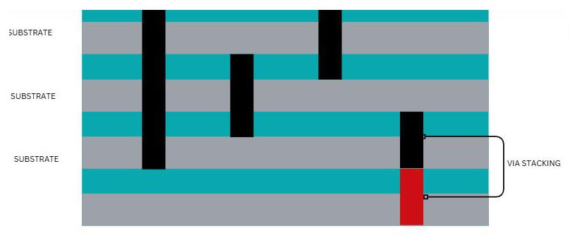
They also have strict aspect ratio limits (usually ≤ 1:1), so deeper connections typically require stacking or staggering.
Designers often place long fanouts or assume microvias can connect directly to deep core layers without intermediate vias — which is not possible.
Laser drilling for microvias requires clear access.
You can’t drill through a solid copper plane on the core layer if it is directly under the via pad (or worse, if the plane blocks the laser path).
Stacking (aligning multiple microvias directly on top of each other) may look good for density, but it becomes a reliability risk when overdone.
Every PCB manufacturer has slightly different capabilities for sequential lamination, including:
- Maximum microvia diameter and depth
- Allowed stacking levels
- Minimum dielectric thickness
- Via fill requirements
- Registration tolerances for sequential steps
1 + N + 1 isn’t just another stackup notation — it has become the industry’s go-to solution for most modern high-density, high-speed, and compact electronic products that don’t justify the added cost and complexity of full any-layer HDI or 2 + N + 2 designs.
When executed correctly — with early fab involvement, realistic via rules, proper plane placement, and a disciplined via strategy — 1 + N + 1 delivers real, measurable benefits:
- Fine-pitch BGA escape down to 0.35–0.5 mm pitch
- Multi-gigabit signal integrity with clean eye diagrams
- Thin, lightweight, and reliable boards
- Reasonable manufacturing cost with solid yield
When done wrong, however, the outcome is predictable: respins, field failures, frustrated customers, and budgets that mysteriously double.
So the next time you start a new design, pause and ask yourself:
- Do I really need more than 1 + N + 1?
- Have I talked to my fabricator before finishing placement?
- Am I treating microvias with the respect they deserve — powerful, but picky?
If you’re looking for a manufacturing partner that understands sequential lamination, HDI constraints, and real-world yield trade-offs, PCBCool works closely with designers from the earliest stackup decisions through volume production.
You’ve got the knowledge now.
Go build something awesome.