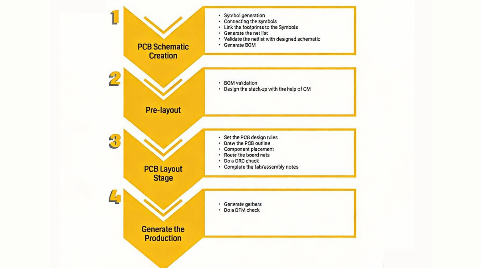
In 2024, I led post-mortems on 53 failed PCB projects. In 41 of these cases, the schematic was correct, the components were authentic, and the layout passed DRC—yet the boards failed in validation. Why? The process was broken, not the output.
Teams skipped stackup validation, routed high-speed signals before defining impedance, and handed off to layout without thermal targets. The result? 3–6 week respin cycles, blown deadlines, and eroded client trust.
This guide delivers the field-proven 7-phase PCB design process used in automotive, medical, and industrial deployments—not as a textbook flowchart, but as a failure-aware sequence with phase gates, validation triggers, and escape hatches.
No theory. Just what survives Nairobi dust, European EMC chambers, and 24/7 industrial operation.
Most teams jump straight to schematics. The best start with system boundaries:
- Electrical: Voltage rails, max current, noise tolerance (e.g., “ADC reference: ±0.5% over 0–70°C”)
- Mechanical: Board dimensions, mounting holes, connector locations
- Environmental: Operating temp, humidity, vibration profile (e.g., “IP65 enclosure, 5–50°C”)
- Regulatory: EMC (FCC/CE), safety (IEC 62368), RoHS
Real Failure:
A solar charge controller passed lab tests—but failed in coastal Kenya. Why? No salt-spray creepage spec. Traces spaced at 0.2 mm shorted at 85% RH.
Deliverable:
System Requirements Document (SRD) – a living spec signed off before Phase 2.
Figure 1: System Requirements Document Template
The schematic isn’t just wires and symbols. It’s the first physical model – if done right.
Critical Practices:
- Hierarchical Blocks: Group power, analog, digital, RF – even in single-sheet designs
- Design Annotations: Add notes like “Keep D+ D− < 100 mm, matched ±0.1 mm” directly on nets
- Power Tree: Show decoupling strategy – bulk → ceramic → IC pin
- Pin-Swapping Planning: Mark swappable pins (e.g., SPI MISO/MOSI) for layout flexibility
Failure Avoided:
A drone flight controller annotated “I²C clock: max 30 cm, no vias”. Layout obeyed – zero bus lockups in 2,000 units.
Validation Gate:
- All ICs have power/ground pins connected (no floating VCC)
- All high-speed interfaces have length/skew notes
- Net classes defined (e.g., POWER, ANALOG, USB_HS)
This is where most projects fail. Skipping this phase turns layout into guesswork.
Must-Have Elements:
- Layer Stackup: Material (e.g., Isola FR408HR), thickness per layer, copper weight
- Impedance Table:
| Net Class | Target Z | Tolerance | Layer | Max Length |
|---|
| USB_HS | 90 Ω | ±10% | L1 | 120 mm |
- Power Integrity: Target impedance, decoupling strategy, plane splits
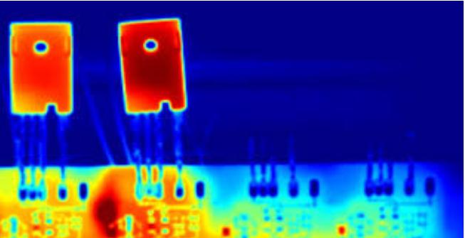
- Thermal Plan: Hotspot IDs, minimum copper area, thermal via count/size
- EMC Zones: Keep-out regions, shielding requirements, grounding strategy
Pro Tip:
Use a 1-page PCB Design Spec – even in startups. If it doesn’t fit, you’re likely overcomplicating the spec.
Placement is not about aesthetics. It is signal integrity, thermal flow, and manufacturability executed at the same time.
Critical Rules:
- Thermal First: Place high-power devices (MOSFETs, regulators) near board edges or dedicated heatsink zones
- Signal Flow: Maintain a clear left-to-right or bottom-to-top path (e.g., antenna → RF → processor → communications)
- Decoupling Proximity: Place capacitors within 2 mm of IC power pins, with vias kept as short as possible
- DFM Compliance:
- Avoid tall components near connectors (can obstruct mating)
- Place fiducials within 10–100 mm of fine-pitch ICs
- Ensure test points are accessible (no vias under RF shields)
Real Cost:
A motor driver placed MOSFETs at the center of the board with no defined airflow path. Field units failed at 48°C ambient, despite components rated for 125°C junction temperature.
Placement Gate Checklist:
- All thermal hotspots have defined heat escape paths
- High-speed ICs (USB, Ethernet) have continuous return paths
- Mixed-signal separation enforced (analog kept >10 mm from switching nodes)
- All test points and fiducials meet assembly and test requirements
Routing is not “connecting dots.” It is the enforcement of physical laws in copper.
Execution Protocol:
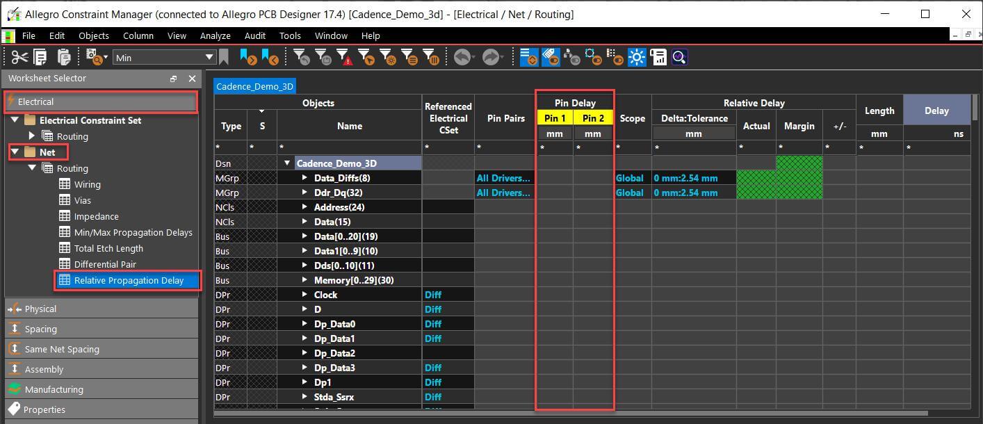
- Import constraints from Phase 3 into the layout tool
- (e.g., Altium Design Rules, Cadence Allegro Constraint Manager)
- Route critical nets first:
- Power Delivery: wide, short paths with low loop inductance
- High-Speed Signals: length-matched, no stubs, controlled impedance
- Analog Signals: guard rings where required, isolated from digital crosstalk
- Apply DFM rules early:
- Minimum trace/space per copper weight (e.g., 0.2 mm for 1 oz copper)
- Teardrops on vias to improve yield
- Avoid 90° bends; use 45° angles or curves
Advanced Practice:
Match signal delay, not just physical length.
For example, a 125 MHz SPI interface may tolerate up to 800 ps skew, which can translate to ~120 mm of trace mismatch depending on stackup — not “the same millimeter length.”
Failure Avoided:
DDR3 lines routed to ±50 ps skew (not ±1 mm). Zero bit errors at 800 Mbps in validation testing.
Passing DRC does not mean the board will function in the real world. True validation goes beyond rule checks and verifies electrical, thermal, and manufacturing behavior.
Validation Should Include:
| Check | Tool | Why It Matters |
|---|
| Signal Integrity | SIwave, HyperLynx | Finds reflections and crosstalk DRC cannot detect |
| Power Integrity | PDN Analyzer | Verifies target impedance across the frequency range |
| Thermal Simulation | Ansys Icepak, SimScale | Predicts hotspots before fabrication |
| DFM Audit | GC-Prevue, FreeDFM | Catches fab-specific issues (e.g., solder mask slivers) |
| Netlist Compare | CAM350, Gerbv | Ensures no unconnected or swapped pins |
Critical:
Run SI and PI analysis only after routing is 100% complete. Partial layouts produce misleading results and false confidence.
Validation Gate (Must Pass All):
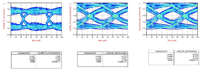
- SI: Eye diagram open at the receiver
- PI: ZPDN < Ztarget up to the maximum frequency of interest
- Thermal: Tjunction below specification with at least a 10°C margin
- DFM: Zero critical violations for the target fabrication house
Exporting Gerbers is not the end of the process. It is the last opportunity to prevent scrap, delays, and misinterpretation on the factory floor.
Handoff Protocol:
- Generate
- Gerbers (RS-274X) for all layers
- NC Drill (Excellon v2)
- IPC-356 netlist (optional, but strongly recommended)
- BOM (CSV + XLSX)
- Validate
- Use tools such as GC-Prevue or FreeDFM to confirm:
- Drill units match Gerber units
- Board outline is closed (no gaps or arcs)
- Solder mask expansion ≥ 0.075 mm
- Package
- ZIP archive with clean naming: ProjectName_YYYYMMDD/
- Include a Readme.txt with:
- Layer stackup
- Impedance requirements
- Special instructions (e.g., “Leaded process required,” “Blue solder mask”)
Real Win:
A Nairobi-based team included the full stackup in the Readme.txt. The fabrication house used the correct material on the first build—resulting in a 98.7% first-article yield.
Deferring thermal, EMC, or power integrity decisions to layout guarantees compromise. Layout can optimize within constraints—but it cannot invent them.
→ Fix: Enforce Phase 3 design specification sign-off. No layout begins without it.
Running signal or power integrity analysis after routing almost always leads to expensive regret.
→ Fix: Simulate critical topologies before routing. Ask questions early, such as:
“Can this USB interface run on Layer 3?”
Placing a 0.4 mm-pitch BGA without accessible test points often results in an untestable board, regardless of electrical performance.
→ Fix: Involve your EMS partner early and obtain their DFM and test requirements before component placement.
The PCB design process isn’t a linear path — it’s a series of gated commitments, each one designed to prevent the next failure mode.
The fastest teams aren’t the ones who route the quickest. They’re the ones who validate intent before execution, document boundaries before handoff, and audit physics before fabrication.
Because in hardware, speed isn’t measured in mm/day — it’s measured in first-article yield and long-term field reliability.
At PCBCool, DFA isn’t treated as a checklist at the end of the process — it’s built into how we support PCBA projects from the start.
Our engineering team reviews design files, assembly constraints, and manufacturing assumptions before production begins, helping identify risks that could impact yield, testability, or assembly flow. This early review allows teams to move from concept to a production-ready PCBA with fewer iterations, fewer surprises, and a smoother path to first build success.