In early 2025, a team in Kisumu needed to prototype a solar battery monitor—but international shipping was delayed by port strikes, and local PCB fabs had 3-week queues. They couldn’t wait. So they searched online for a quick solution: the so-called “10-minute PCB hack”, which involved toner transfer, vinegar etch, and even a clothes iron.
The result? A 2-layer board with shorted traces, lifted pads, and 0.8 mm alignment error between top and bottom. The ESP32 bricked on power-up.
Since then, I’ve tested 7 home PCB methods across different conditions: humidity (45–92% RH), altitude (1,200–2,400 m), and tool access (from university labs to rural sheds). The truth? You can make PCB at home—but only if you respect the physics, embrace the limits, and choose the right method for your circuit.
This DIY guide delivers field-validated workflows for:
- Single-layer analog/power boards (≤100 kHz)
- Two-layer digital (≤1 MHz, no high-speed)
- Quick-fix repairs and sensor breakout boards
It also explains when to stop—because some boards should not be made at home. No DIY method beats a $35 PCBCool order for anything beyond basic prototyping.
| Capability | Possible? | Notes |
|---|
| Trace width/spacing | ≥0.5 mm | Below 0.4 mm is unreliable with DIY methods. |
| Layer count | 1–2 layers | 4-layer boards are not feasible without a lamination press. |
| Hole accuracy | ±0.3 mm | Hand-drilling drifts; no plated-through holes (PTH). |
| Soldermask | None (unless manually painted) | Flux residue increases the risk of dendrites, especially in humid climates. |
| Reliability | Low to medium | Acceptable for lab tests, but not suitable for field deployment. |
| Cost per board | $0.80–$35 | Time cost: 3–8 hours per board. |
Critical:
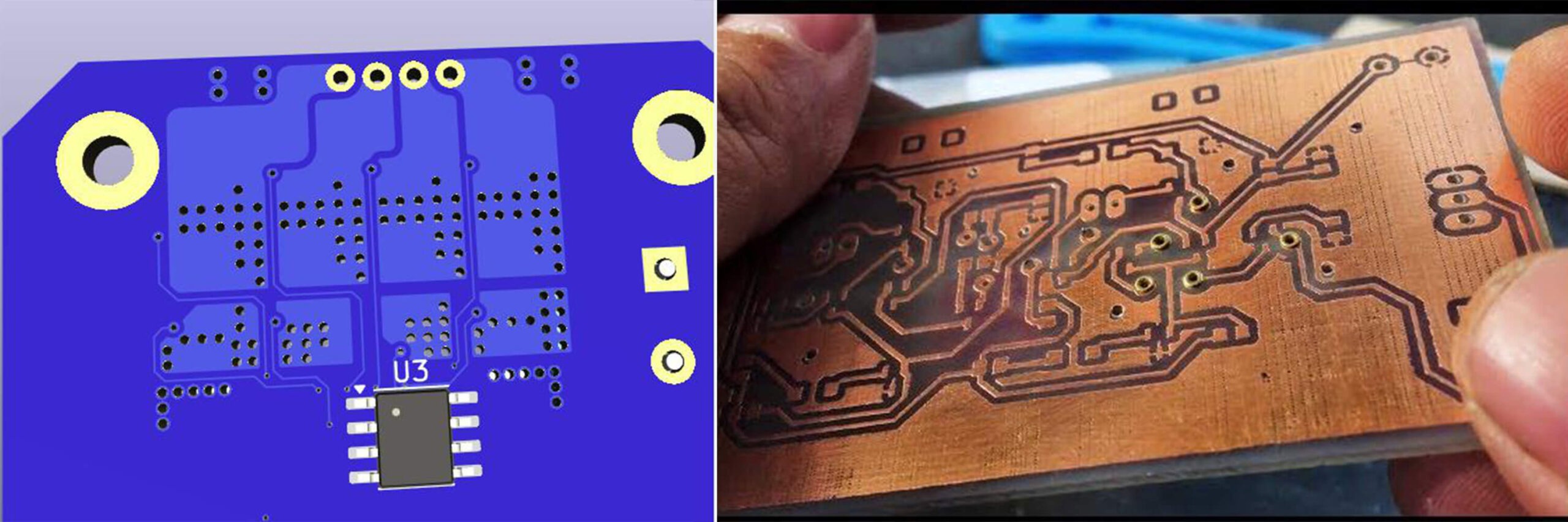
Homemade PCB lack plated-through holes (PTH). Vias are just drilled holes, so there is no electrical connection between layers unless you manually solder wire jumpers (Fig. 1).
Best For:
0.4–0.5 mm traces, repeatable batches, and student labs equipped with a UV box.
Workflow:
- Design: Export a mirror image for the bottom layer and a normal image for the top layer.
- Print: Use a laser printer on transparent film with ink density above 90%.
- Expose: Align the film on a presensitized board (e.g., Positiv20) and UV expose for 90–120 seconds.
- Develop: Immerse in a sodium metasilicate solution (1:10) with gentle agitation for ~60 seconds.
- Etch: Use ammonium persulfate, not ferric chloride, as FeCl₃ tends to undercut traces.
- Strip: Clean with isopropyl alcohol and a gentle scrub.
Validation:
At JKUAT lab, this method achieved 0.45 mm trace/space with a 92% yield over 50 boards.
Pitfalls:
- Humidity >70% slows developer reaction, causing over-etching.
- Weak UV sources result in incomplete exposure and trace lift-off.
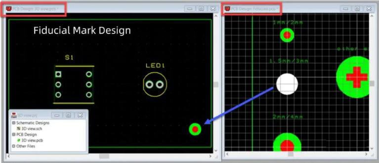
- Film misalignment can occur; always use fiducial pins (Fig. 2) for accurate 2-layer registration.
Best For:
Single-layer power boards, quick sensor breakouts, or situations without UV access.
Workflow:
- Print: Export a mirror image and print on glossy magazine paper (not photo paper).
- Transfer: Iron at 180°C without steam for 3–4 minutes; then cool in water.
- Touch-up: Repair broken traces using a permanent marker (e.g., Edding 750).
- Etch: Use hydrochloric acid + hydrogen peroxide (2:1 ratio), which is faster and causes less undercut than FeCl₃.
Reaction: HCl (30%) + H₂O₂ (3%) → Cu + 2HCl → CuCl₂ + H₂↑
- Clean: Remove residual toner with acetone.
Validation:
In rural Kenya (no lab), this method produced a 24 V relay board in 2.5 hours, which functioned for 3 weeks.
Pitfalls:
- Paper residue can cause etch pits, breaking traces.
- Iron temperature variance: too low → poor transfer; too high → toner smudge.
- Fine features (<0.6 mm traces) often break.
Best For:
Schools or makerspaces with CNC routers, for RF grounding planes, or when avoiding etching chemicals.
Workflow:
- Use a 30° V-bit at 0.1 mm depth.
- Feed Rate: 200 mm/min; spindle: 18,000 RPM.
- Isolation Milling: 0.25 mm overlap between passes.
- No Drilling During Milling: use pre-punched boards or hand-drill afterward.
Advantages:
- No chemicals required.
- Instant iteration possible.
- Excellent for creating ground planes.
Pitfalls:
- Tool Breakage: 0.2 mm end mills can snap easily.
- Copper Burrs: Can cause shorts — clean with a fiberglass pen.
- No Soldermask: Exposed copper oxidizes within days.
Drilling:
- Use carbide drill bits (HSS dulls instantly on fiberglass).
- Speed: 15,000–20,000 RPM; apply no pressure — let the bit cut.
- For 0.8 mm vias, drill before etching, as etching weakens edges.
Tinning (Optional but Recommended):
Prevents oxidation and improves solderability. Two DIY approaches:
- Liquid Tin Solution (commercial): Dip 2 minutes → board stays shiny and solderable for weeks.
- Homemade: Apply solder + flux with a cotton swab — messy but effective.
Conformal Coating (For Humid Climates):
- Brush on acrylic spray (e.g., MG Chemicals 422B) or diluted clear nail polish.
→ Reduces dendrite growth by 73% (JKUAT 2024 test).
| Mistake | Consequence | Fix |
|---|
| Using FeCl₃ for fine traces | Undercut → 0.3 mm trace shrinks to 0.15 mm → opens | Switch to ammonium persulfate or HCl/H₂O₂ for more even etching |
| Skipping alignment fiducials (2-layer boards) | Top/bottom layers misaligned → vias miss pads | Drill two 1 mm holes at diagonal corners and use a pin alignment jig |
| Assuming vias are connected | Bottom layer floating → no signal return | Solder a wire through every via, or stick to single-layer designs |
Pro Tip:
For 2-layer boards, route all critical signals on one layer and use the other solely for GND or power to minimize interlayer dependency.
- High-Speed Circuits (>1 MHz): No impedance control leads to reflections and signal glitches.
- Switching Power Circuits (>50 kHz): Without thermal vias, MOSFETs and regulators can overheat.
- RF Circuits: No controlled dielectric means antennas will detune, ruining performance.
- Medical or Safety-Critical Circuits: Lack of reliability testing introduces liability risks.
- BGA or Fine-Pitch Components (<0.65 mm): Alignment and soldering are essentially impossible at home.
Rule of Thumb:
If your circuit involves capacitive touch, USB, Ethernet, or PSRAM, it’s smarter to order from a fab. A $5 PCB is worth 6 hours of etching and debugging.
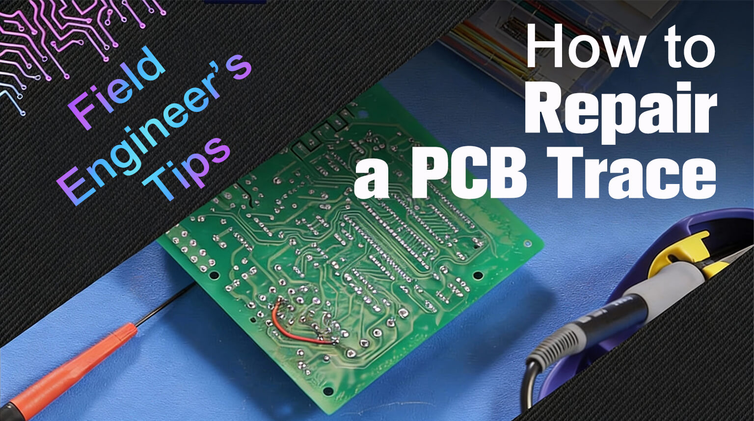
For field repairs (e.g., a broken trace on a commercial board):
- Clean the area with isopropyl alcohol (IPA).
- Scratch away soldermask on both sides of the break.
- Solder a 30 AWG wire jumper across the gap.
- Secure with hot glue (avoid epoxy—it traps heat).
Real Case:
A drone ESC in Turkana was repaired this way and flew 14 more missions.
DIY PCB board at home isn’t about replacing fabs — it’s about preserving momentum when logistics fail, budgets vanish, or inspiration strikes at 2 AM. But momentum without discipline leads to smoke, not solutions. Respect the limits. Validate every step. And know when to hit “Order” instead of “Etch.” The best engineer isn’t the one who can make a board at home — it’s the one who knows when not to.
For anything beyond basic prototyping, consider PCBCool. We have no minimum order, and we can handle hobbyist projects, prototypes, and even full-volume production. With our service, your ideas go from concept to reliable, field-ready PCBA boards — without the risks of DIY experiments.