Most contract assemblers treat post-reflow cleaning as a checkbox — ultrasonic, spray, vapor, it all removes flux residue. And for resistors, capacitors, and standard ICs, that is true.
But MEMS sensor board assembly plays by different rules. The moment a board carries devices with free-standing mechanical microstructures measured in single-digit microns, standard cleaning becomes destructive.
A US satellite education company found out the expensive way: 15% of their sensor boards came back dead from their previous assembler’s ultrasonic line. PS Electronics delivered the same boards with zero sensor damage — and handled the EOL component sourcing for the discontinued IMU chip to do it.
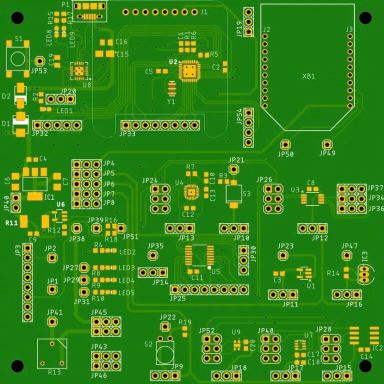
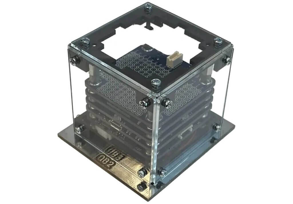
The client develops hands-on satellite education kits used in university aerospace engineering programs. Their flagship product is a sensor-dense circuit board that replicates the telemetry subsystem of a CubeSat.
It is worth mentioning that the company was founded by a figure credited with co-inventing the CubeSat standard, and its curriculum is adopted by programs affiliated with NASA and major defense contractors.
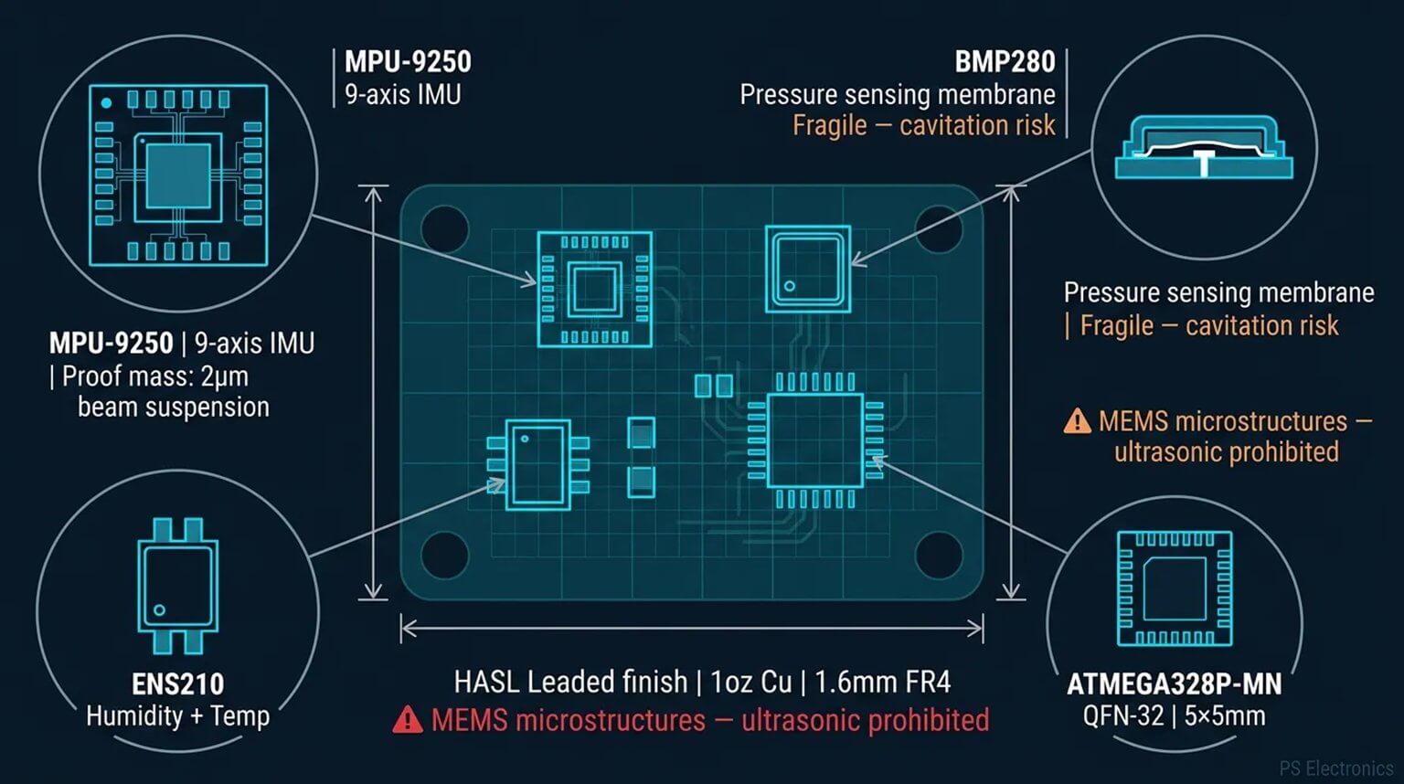
The board packs four sensitive components into a compact 1.6 mm FR4 substrate:
- an MPU-9250 (9-axis IMU combining accelerometer, gyroscope, and magnetometer)
- a BMP280 barometric pressure sensor
- an ENS210 humidity and temperature sensor
- an ATMEGA328P-MN microcontroller in a 5×5 mm QFN-32 package
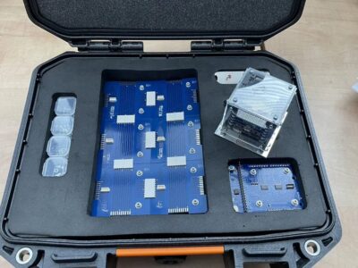
The design also includes rows of through-hole pin headers so students can connect the board to breadboards and external instruments.
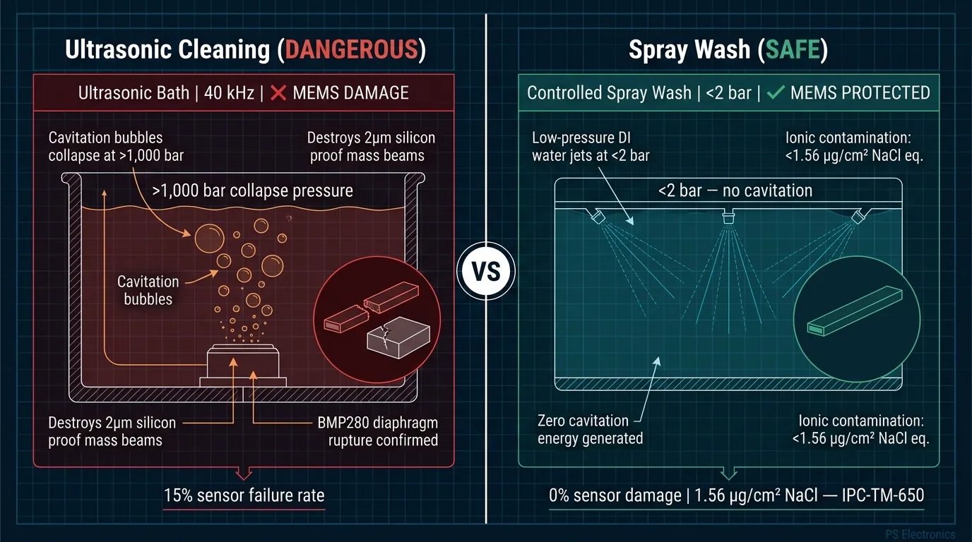
The previous supplier treated this as a routine consumer-grade PCBA. They ran the boards through a standard ultrasonic cleaning bath operating at 40 kHz after reflow. The result:
15% of boards failed the incoming test.
Post-mortem analysis showed fractured suspension beams inside the MPU-9250 and ruptured diaphragms in the BMP280. Cavitation energy from the ultrasonic transducer had destroyed the mechanical sensing elements that give these components their function.
The problem was compounded by a supply chain constraint. InvenSense (now TDK) had discontinued the MPU-9250. Every damaged unit meant burning through irreplaceable inventory.
The client needed a turnkey PCBA partner who understood three things simultaneously:
- Why you cannot clean MEMS boards the same way you clean everything else
- How to handle EOL component sourcing for discontinued silicon
- How to run leaded solder in a RoHS-dominant supply chain — because the client specified HASL with lead for teaching solderability.
The fix started with removing the ultrasonic bath entirely.
Here is why. Ultrasonic cleaning generates cavitation bubbles that collapse with localized pressures exceeding 1,000 bar. The proof mass inside the MPU-9250 is suspended on silicon beams roughly 2 um wide. The BMP280 pressure-sensing membrane is similarly fragile.
These structures do not survive cavitation. There is no “gentle” ultrasonic setting that changes this — the physics is the physics.
PS Electronics replaced the bath with a controlled spray-wash system using deionized water jets at less than 2 bar. The low-pressure spray dislodges flux residue from pad surfaces and under low-standoff components without generating cavitation energy.
Post-wash ionic contamination measured below 1.56 ug/cm2 NaCl equivalent per IPC-TM-650 — same cleanliness standard as ultrasonic, without the collateral damage.
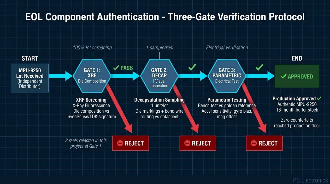
Sourcing the discontinued MPU-9250 required working with independent distributors outside the authorized channel. Every incoming reel passed through a three-gate authentication protocol:
- X-ray fluorescence (XRF) to verify die composition matched the InvenSense/TDK material signature.
- Decapsulation sampling — one unit per lot, chemically decapped to visually confirm die markings and bond wire routing against the reference datasheet.
- Electrical parametric testing — each sampled unit bench-tested against known-good reference units for accelerometer sensitivity, gyroscope bias, and magnetometer offset.
Two suspect reels were rejected during the sourcing phase based on XRF anomalies. The remaining verified stock was sufficient to establish an 18-month supply buffer.
The board combines surface-mount QFN and MEMS packages with through-hole pin headers — a mixed-technology design that requires two solder processes.
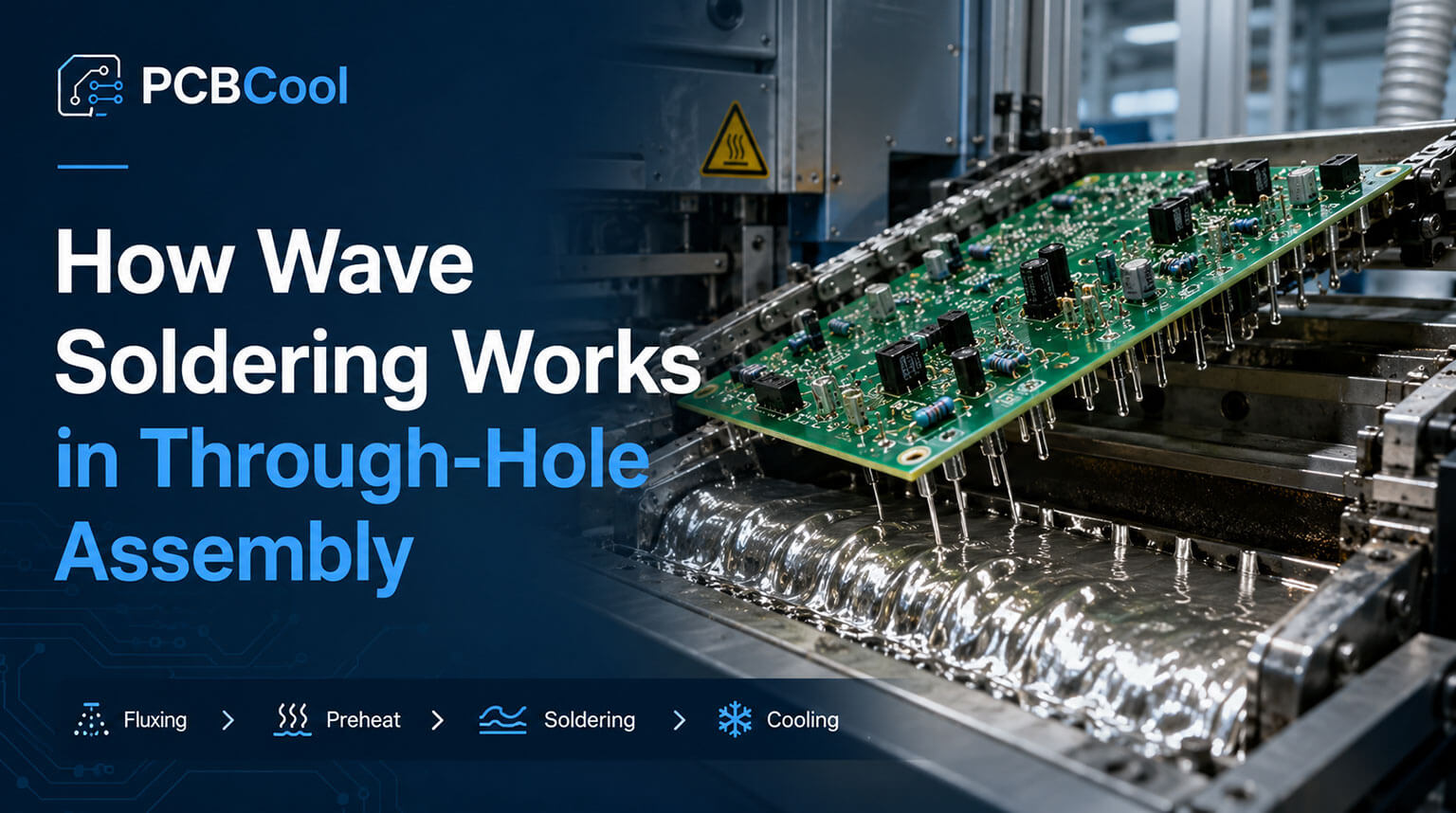
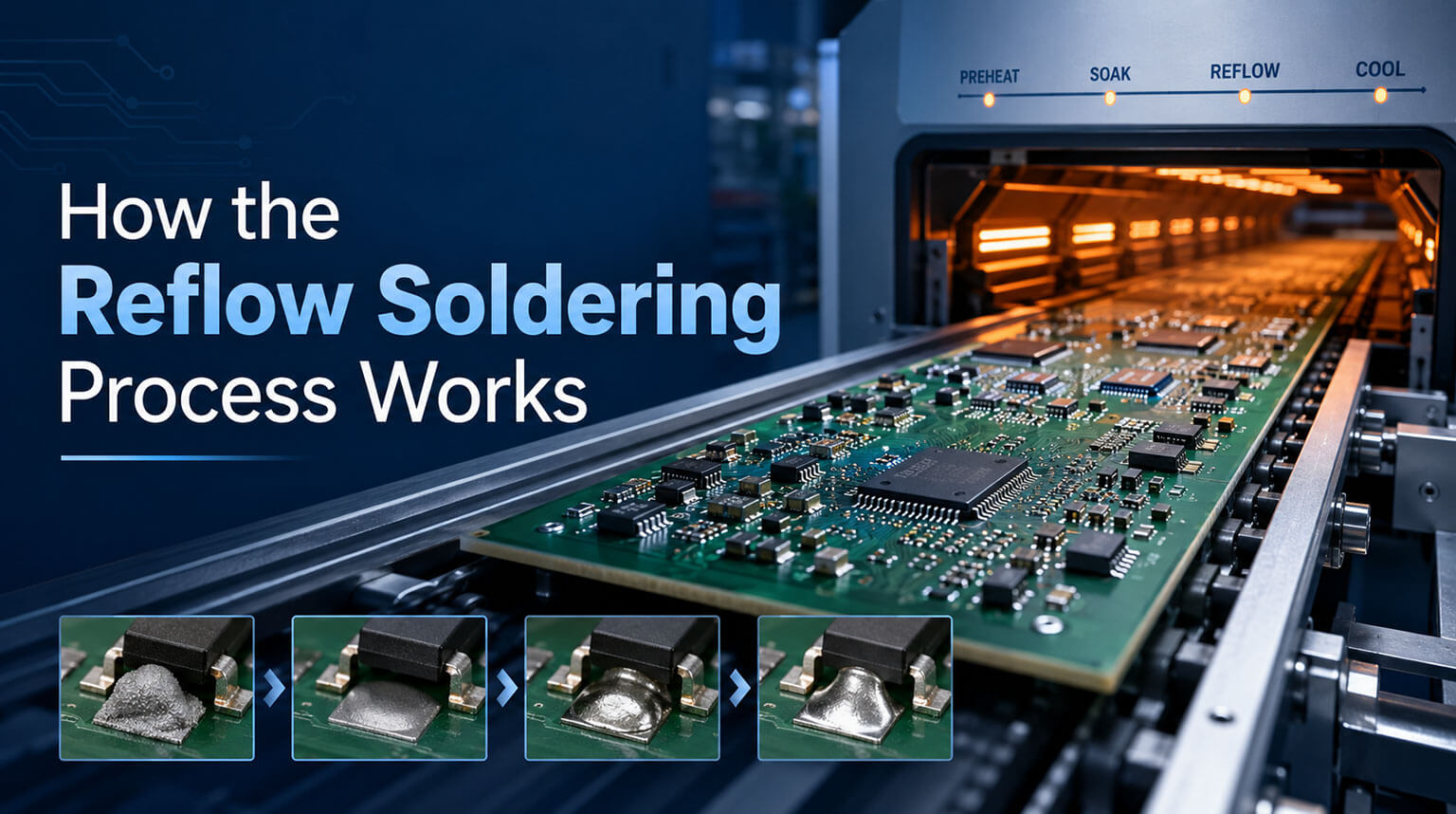
PS Electronics ran SMT reflow first using a Sn63Pb37 leaded profile with peak temperature at 230 C. The through-hole headers were then attached via selective wave soldering.
Why selective and not a second reflow pass? Because running the whole board through another 230 C cycle would re-expose the MEMS devices to peak thermal stress.
Selective soldering kept the topside board temperature below 150 C — well within the MEMS manufacturers’ recommended limits.
- MEMS Sensor Integrity: 100% functional pass rate across all delivered batches. Zero cavitation-related damage. Each board’s IMU self-test register returned nominal values; BMP280 barometric readings fell within +/-1 hPa of reference; ENS210 humidity response tracked within specification. This compared against the previous supplier’s 15% failure baseline.
- EOL Component Quality: 100% lot acceptance after the three-gate XRF, decap, and parametric screening. Two suspect reels were caught and rejected at the XRF gate — before they ever touched the production floor. That is the point of front-loading authentication: you find the fakes at incoming, not at functional test.
- Turnkey PCBA Yield: First Pass Yield of 98.7% on the SMT stage and 99.2% on the DIP stage. Defects were limited to minor solder bridging on non-critical test points, corrected by touchup before functional test.
- Leaded Surface Finish: HASL with lead verified per J-STD-003 wetting balance test, confirming the surface finish met the client’s requirement for student hand-soldering compatibility in downstream lab exercises.
The QC plan was designed around two facts: MEMS devices cannot tolerate mechanical probe contact, and EOL components require authentication before they touch a production line.
- IQC (Incoming Quality Control): Every EOL component lot underwent 100% XRF screening plus visual inspection under 20x magnification for remarking indicators (sanding marks, inconsistent font, pin oxidation patterns). Parametric bench testing against golden reference units served as the final gate. Standard BOM components were verified against manufacturer date codes and moisture sensitivity levels.
- IPQC (In-Process Quality Control): Solder paste inspection (SPI) verified deposit volume on all QFN pads before component placement. AOI (Automated Optical Inspection) after reflow was configured with MEMS sensor exclusion zones — the optical system flagged joint defects without applying mechanical probe pressure to the sensor packages. After the spray-wash cycle, ionic contamination testing confirmed residue levels below the IPC-TM-650 threshold of 1.56 ug/cm2 NaCl equivalent.
- OQC (Outgoing Quality Control): 100% functional testing included IMU self-test register verification, barometric pressure calibration check (+/-1 hPa), and humidity sensor response validation. Boards were packaged in ESD-safe trays per ANSI/ESD S20.20, critical for a bare-board satellite education product that students handle directly.
The process runs under PS Electronics’ ISO 9001 and ISO 14001 certified quality management system.
PS Electronics delivered the initial production batch in 8 working days from materials receipt. The boards entered classroom use the following semester with zero field failures reported.
The verified EOL sourcing pipeline established an 18-month buffer stock of authenticated MPU-9250 units, eliminating the single biggest supply chain risk on their BOM. By consolidating PCB fabrication, component procurement, and PCBA into a single turnkey relationship, the client eliminated management overhead across three separate vendors.
The Project Lead summarized the outcome:
We spent two years dealing with suppliers who treated our MEMS boards like standard consumer electronics. The first batch came back with 15% sensor failures from their cleaning line. PS Electronics understood that these sensors have mechanical microstructures inside — they engineered the process around that constraint instead of forcing our board through a standard line.
The project runs as a recurring production engagement. PS Electronics manages both the assembly and the ongoing EOL component pipeline — the client does not source a single part themselves.
If your design includes MEMS sensors, pressure membranes, or other mechanically sensitive devices, contact PS Electronics for a DFM review before your next sensor board assembly. The cleaning process matters more than most engineers expect.