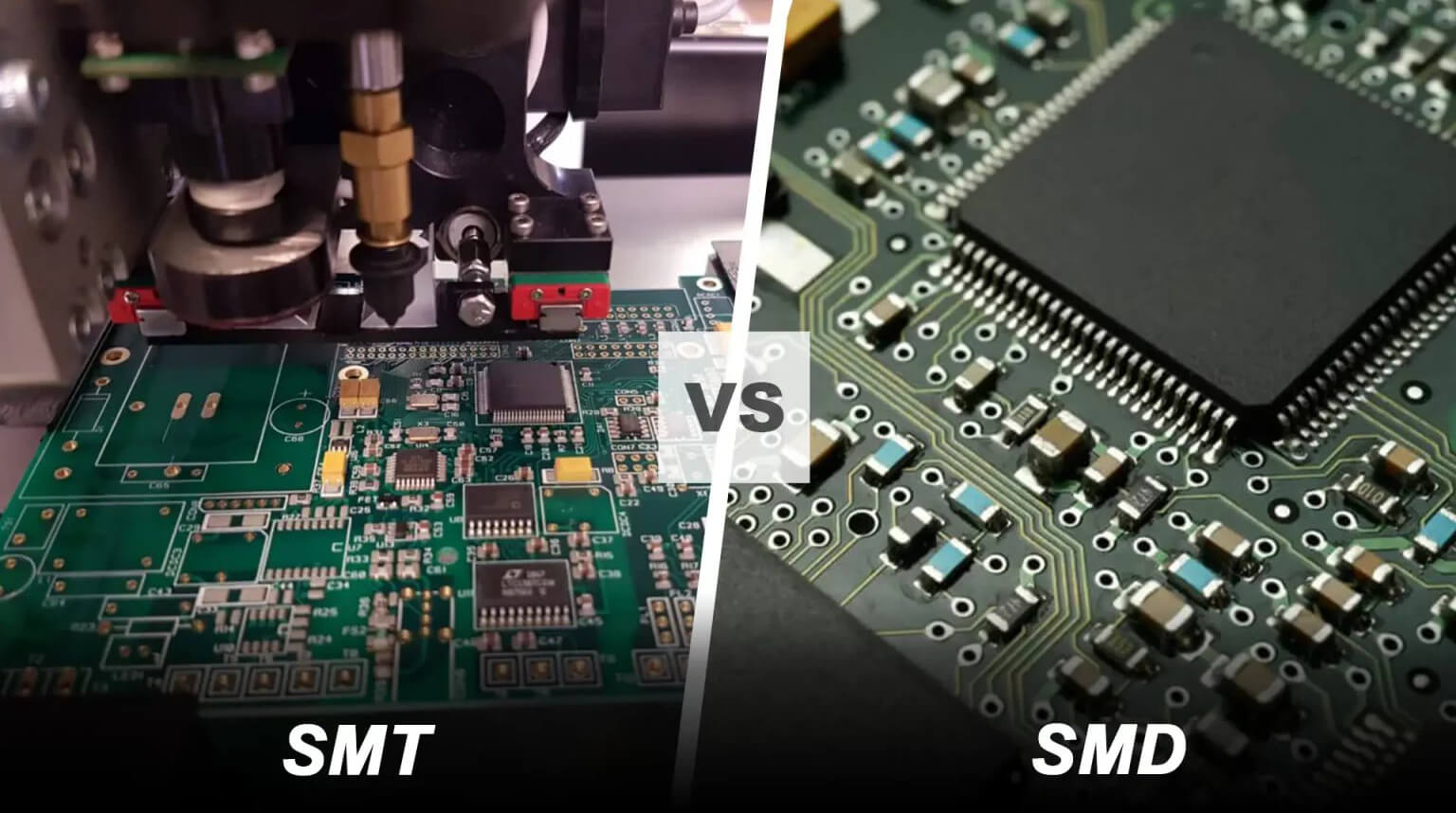
As electronic products continue to get smaller and more powerful, Surface Mount Devices (SMD) have become the norm, driving the electronics manufacturing industry into the era of Surface Mount Technology (SMT). Delivering precise, efficient placement of SMD components has become a critical benchmark for an EMS provider’s technical expertise and production performance.
Unlike traditional hand soldering, professional SMT assembly isn’t just a single step—it’s a fully standardized, closed-loop process that includes preparation, core production, quality control, and post-processing. Each stage follows strict process guidelines, requires specialized equipment, and adheres to measurable quality standards.
This guide takes you inside a real EMS production environment. Following industry standards such as IPC-A-610J (Acceptability of Electronic Assemblies) and IPC J-STD-001J (Requirements for Soldered Electrical and Electronic Assemblies), and drawing on years of hands-on SMT mass-production experience, PCBCool provides a complete breakdown of the SMT assembly process. The process parameters and operating specifications shared here come straight from real-world production lines—not theoretical labs—offering practical insights that engineers and procurement professionals can actually use.
Based on over 20 years of PCB project experience, we’ve found that roughly 70% of production issues trace back to the early design and preparation stages. To tackle this, we’ve optimized our workflow: from the moment a customer inquiry comes in, our engineering team proactively engages in DFM (Design for Manufacturability) collaboration to ensure the design is fully aligned with SMT process requirements.
Key DFM considerations during PCB design include:
- Pad Design: Following IPC-7351 standards, pad dimensions and spacing are tailored to the component package. For example, 0402 resistor pads are typically 1.0mm × 0.5mm ±0.05mm, while BGA pads need precise ball diameter matching and space for X-ray inspection.
- Reference Points (Mark Points): Alignment reference points are placed at opposite corners of the PCB (at least two points, 1.0–2.0mm in diameter), with no nearby components or silkscreen within 3mm.
- Component Layout: Similar components are oriented consistently. High-power components are distributed away from temperature-sensitive devices. Fine-pitch components are placed at least 3mm from board edges, with minimum spacing of 0.3mm (precision ICs ≥0.5mm).
- Thermal Management: High-power components use thermal pads and vias (≤0.3mm) along with solder mask openings to help dissipate heat effectively.
- Process Edge Design: Reserve 5–10mm process edges on both sides of the PCB and alignment holes of 3.0mm ±0.1mm. Boards without process edges require dedicated fixtures.
During BOM review, our material engineers work with DFM engineers to evaluate customer-provided BOMs for compatibility, procureability, and compliance:
- Material Compatibility: Verify component-to-pad fit and solder paste/flux compatibility.
- Material Procureability: Identify obsolete or hard-to-find parts, suggest alternatives, and flag moisture-sensitive components (MSL ≥3) with proper storage and baking requirements.
- Material Standard Compliance: Confirm model and specs, note packaging format (tape-and-reel, tray, bulk). Tape-and-reel parts follow EIA-481 standards; tray parts comply with JEDEC standards.
Once complete, PCBCool generates a DFM optimization report and BOM review report, highlighting design flaws and recommending corrective actions. Since implementing this workflow, SMT line defect rates have dropped by roughly 60%, saving clients about 30% on redesign costs.
Top-tier SMT assembly factories integrate Incoming Quality Control (IQC) into their overall quality management systems to ensure every batch of materials meets strict standards before hitting the production line.
Sampling typically follows the AQL 1.0 standard (GB/T 2828.1), with inspection procedures tailored to different types of materials.
- Appearance: Boards must be free of scratches and oxidation, with clean surfaces. Solder mask thickness should be 10–25μm, without peeling or bubbles. Silkscreen should be crisp and legible. Pads must be oxidation-free (ENIG gold ≥0.1μm). Board warpage ≤0.5% (for 1.6mm thickness, <0.2mm/m).
- Dimensions: Measured using calipers or a microscope/projector. PCB length/width ±0.1mm; pad size ±0.05mm; mark point size/position ±0.05mm; via hole diameter ±0.1mm, position ±0.05mm.
- Electrical Performance: Flying probe tests for continuity (≤50mΩ) and insulation (≥10¹²Ω) prevent opens or shorts. Multilayer and HDI boards are checked for layer alignment (≤0.05mm).
- Packaging: Boards are vacuum-packed with desiccant and humidity indicator cards (≤10% RH). Shelf life is 6 months; once opened, placement should occur within 48 hours, otherwise baking is required.
- Appearance: Pins must be shiny and free from oxidation or damage. Packages should not be cracked or broken. Tape packaging intact, components securely held.
- Dimensions: Components must match datasheet specs (e.g., 0402 resistor 1.0 × 0.5mm ±0.1mm). Pin spacing (QFP 0.4mm ±0.02mm) and coplanarity (QFP/BGA ≤0.1mm) must comply.
- Electrical Performance: 1% of components sampled for resistance, capacitance, or diode conductivity within datasheet tolerances. Chips checked for visual defects, pin integrity, and functionality if needed.
- Solderability: 10 components immersed in 245℃ lead-free solder for 5s; solder wetting ≥90%, no cold joints or lift-off. Moisture-sensitive components (MSL 3) are baked at 125℃ for 24h if previously opened.
- Appearance: Paste should be smooth, evenly colored, with no clumps or darkening. Labels must indicate model, production date, and shelf life. Unopened paste stored at 5–10℃; shelf life 6 months.
- Viscosity: Measured at 25℃ using a rotational viscometer (Brookfield DV2T). Lead-free paste: 200–300 Pa·s ±10%.
- Metal Content: 10g melted at 250℃; target metal content 40–50%.
- Shelf Life After Opening: 20–25℃ shelf life 24h; stir for 3–5 minutes before use to ensure uniformity, with no sedimentation.
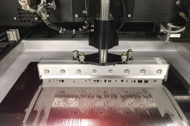
Solder paste printing is one of the most critical steps in SMT assembly. Its main goal is to evenly deposit solder paste onto PCB pads, providing a stable foundation for component placement and reflow soldering, and ensuring high-quality solder joints. Here’s how it works:
- PCB Loading: PCBs are transported to the stencil printer using AGVs (Automated Guided Vehicles) and move continuously along the conveyor system, flowing seamlessly into subsequent SMT processes until assembly is complete.
- PCB Alignment: The printer’s CCD vision system automatically detects the PCB’s reference points for precise alignment, with positioning accuracy within ±10μm. The platform height is adjusted to ensure close contact between the PCB and stencil, maintaining a gap of ≤0.02mm.
- Solder Paste Application: Well-mixed solder paste is evenly applied over the stencil, ensuring all openings are fully covered.
- Automatic Printing: The printer executes the printing motion according to preset process parameters, including squeegee angle, speed, pressure, and separation speed. The squeegee moves at a consistent speed, pressing the paste through stencil openings and depositing it uniformly onto PCB pads.
- Separation (Demolding): After printing, the stencil is lifted from the PCB at a controlled speed of 0.5–3mm/s, preventing smearing or bridging of the solder paste.
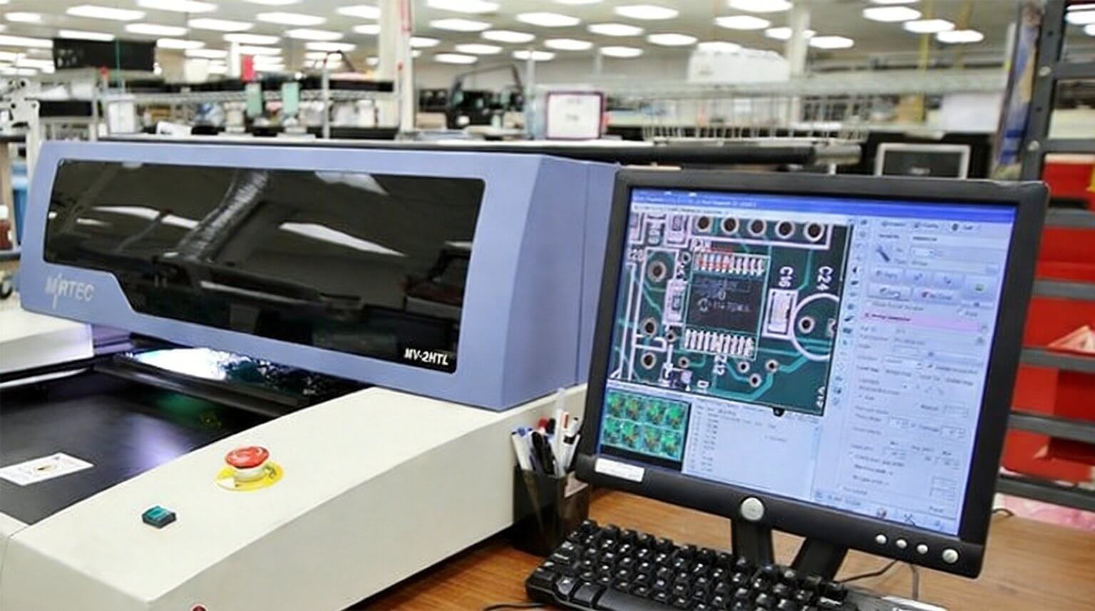
Solder Paste Inspection (SPI) is a crucial quality control step immediately following solder paste printing. Using moiré fringe optical scanning technology, SPI performs 100% inspection of every PCB, accurately detecting printing defects that could affect solder joint quality. Here’s how it works:
- Template Loading: The SPI system automatically identifies the PCB model and loads the corresponding solder paste inspection template.
- Automated Scanning: High-resolution optics scan all PCB pad areas, capturing key data such as solder paste thickness, area, volume, position, and shape. This data is compared in real-time against preset process standards to ensure consistency.
- Defect Evaluation: The system automatically evaluates whether solder paste meets quality requirements. Any anomalies are flagged with defect location and type, trigger alarms, and are uploaded to the MES system for traceability and corrective action.
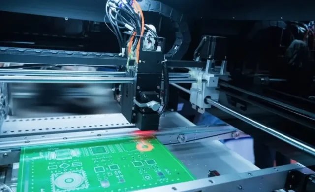
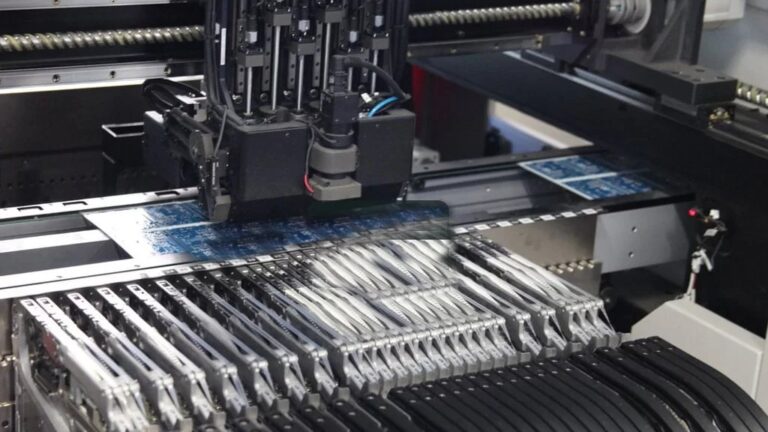
Component placement is the process of accurately positioning SMD components—resistors, capacitors, ICs, connectors, and more—onto PCB pads. It’s one of the most critical steps in SMT assembly, demanding the highest levels of precision in both equipment and process control. Here’s how it works:
- Component Pickup: The placement head moves to the feeder location according to the program and uses vacuum nozzles of the appropriate size to pick up components. After pickup, the vision system checks and corrects the component’s position, rotation, and polarity to ensure accuracy.
- Component Placement: Once calibrated, the placement head moves the components to their target pads at high speed, placing them carefully on the solder paste with precise height and pressure.
- Multi-Head Coordination: Advanced placement machines—such as the Siemens X series—feature multiple placement heads that can pick and place different component types simultaneously, dramatically improving throughput and production efficiency.
By combining high-resolution imaging with advanced algorithms (including deep learning in modern systems), AOI performs 100% inspection of every PCB to verify placement accuracy before reflow. Here’s how the process works:
- Template Loading: The system automatically identifies the PCB model and loads the corresponding inspection program and parameter set.
- Automated Scanning: AOI cameras scan the PCB from multiple angles, capturing data on component position, polarity, rotation, and overall appearance. This data is then compared against predefined standards in real time.
- Defect Evaluation: The system automatically determines whether placement meets quality requirements. Any defects are flagged with location and type, trigger alarms, and are uploaded to the MES system—linking PCB batch, machine, and operator data for full traceability and process analysis.
- Manual Reinspection & Handling: PCBs flagged by AOI are reviewed by operators, typically using high-magnification microscopes (up to 50×) to closely examine suspected defects. Based on the findings, operators may confirm or dismiss defects, fine-tune machine parameters, resolve feeder issues, and re-run production if necessary.
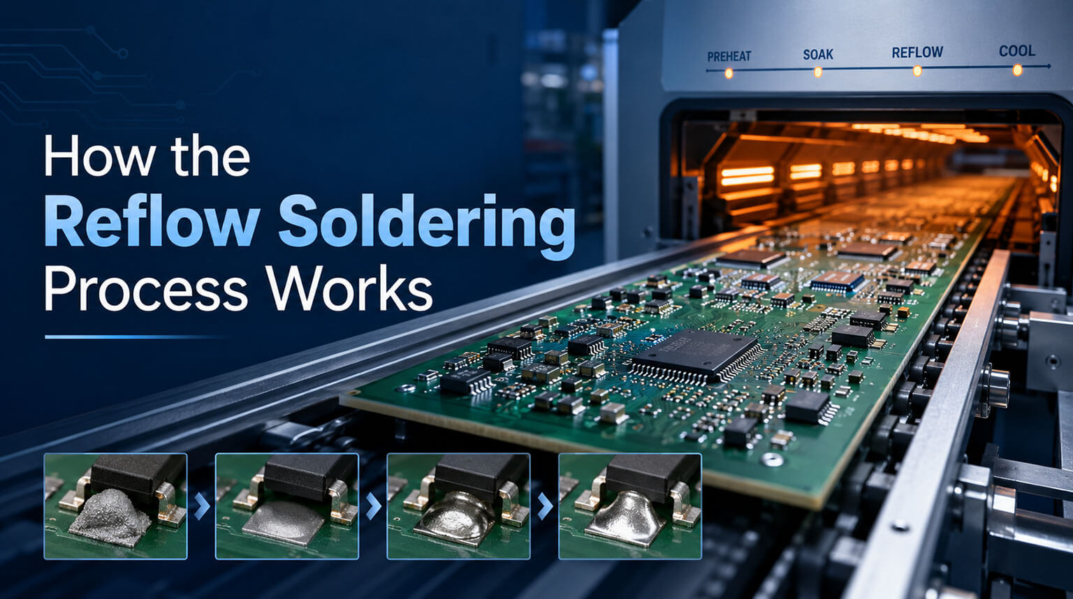
Reflow soldering is where everything comes together. The assembled PCB passes through a reflow oven following a carefully controlled temperature profile, allowing the solder paste to melt, wet the pads and component leads, and then solidify into reliable solder joints during cooling. As one of the most critical steps in SMT assembly, solder joint quality has a direct impact on both electrical performance and long-term reliability. All results must meet IPC J-STD-001J standards.
Here’s what happens during the process:
- Temperature Profile Control: The reflow oven operates based on a predefined temperature profile tailored to the solder paste and component characteristics. PCBs move through four key zones—preheat, soak, reflow, and cooling—guiding the solder paste through a controlled solid → liquid → solid transition.
- Process Monitoring: Operators continuously monitor key parameters in real time, including zone temperatures, conveyor speed, and—when applicable—nitrogen flow and oxygen levels. Any deviation (such as ±2°C temperature drift or conveyor irregularities) triggers an alarm and pauses production for immediate correction.
- PCB Unloading: After reflow, boards are automatically conveyed to the exit. Operators wearing ESD-safe gloves transfer the PCBs into anti-static trays, avoiding direct contact with solder joints to prevent contamination or damage.
- Batch Traceability: Critical process data is recorded for every batch, including temperature profiles, cycle time, nitrogen usage (if applicable), and yield results.
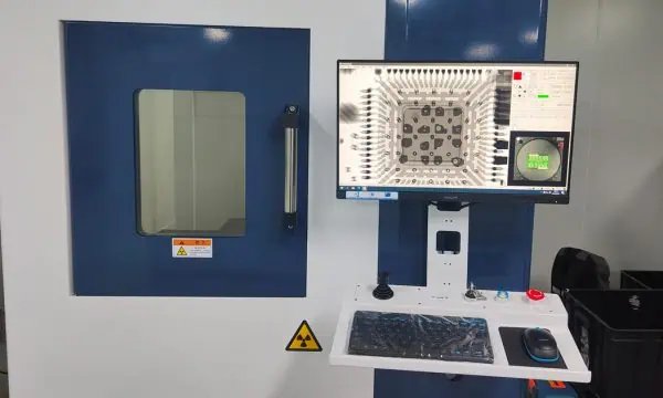
X-ray inspection is a non-destructive technique used to examine hidden solder joints in packages like BGAs, QFPs, and CSPs. Because these connections are not visible to AOI or the naked eye, X-ray inspection plays a critical role in detecting internal defects—especially in high-reliability applications such as automotive, medical devices, and premium consumer electronics.
Here’s how the process works:
- PCB Positioning: PCBs are placed on the X-ray inspection platform using dedicated fixtures to ensure stability and proper coverage of critical component areas.
- Parameter Setup: X-ray intensity and inspection angles (typically adjustable from 0–90°) are configured based on board thickness and component type. The appropriate inspection program is loaded, along with predefined defect criteria.
- Automated Scanning: The system scans the PCB and generates detailed images of internal solder structures. Advanced image analysis algorithms identify defects such as voids, cold joints, solder bridges, and insufficient solder. The system also flags defect locations and calculates key metrics like void ratio and solder fill rate.
- Manual Verification: Operators review flagged areas, adjusting viewing angles or magnification as needed. In some cases, suspected defects are cross-checked using microscopes to minimize false positives.
- Inspection Records: Inspection data for each PCB—including defect type, void ratio, solder fill rate, and inspection time—is recorded to generate a complete report for traceability and quality audits.
SMT assembly isn’t just a sequence of machines and processes—it’s a tightly controlled system where design, materials, equipment, and quality control all have to work together. The difference between a reliable product and a problematic one often comes down to how well each of these steps is executed and managed.
For engineers and product teams, understanding this workflow isn’t just helpful—it’s essential for making better design decisions, reducing risk, and getting products to market faster.
At PCBCool, we specialize in delivering end-to-end SMT assembly services built around real production experience—not theory. From early-stage DFM collaboration to final inspection and quality assurance, our team works closely with customers to ensure every design is manufacturable, every process is optimized, and every board meets strict reliability standards.