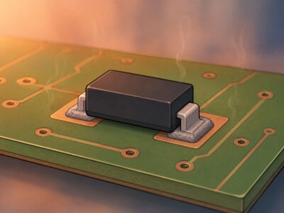
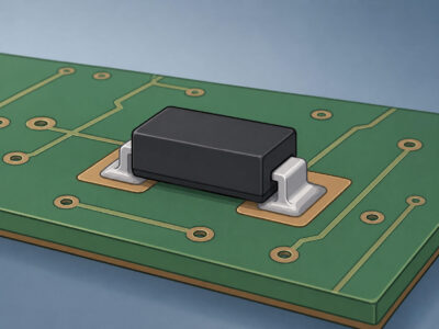
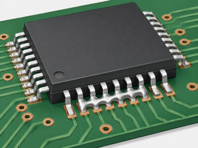
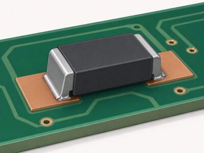
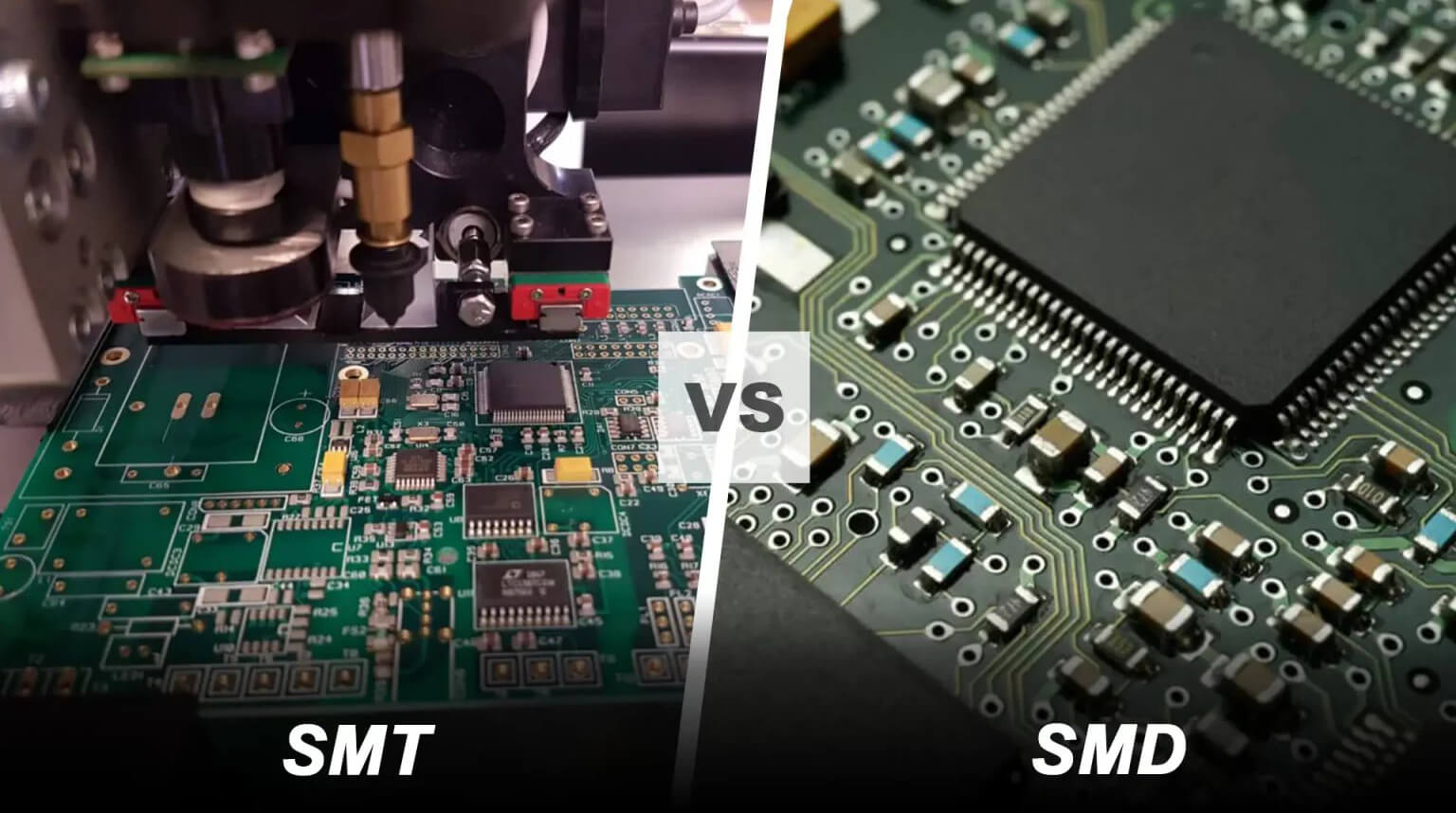
If you open almost any modern electronic product today, you will likely find a PCBA populated with many SMD components. These small surface-mount devices are one reason electronic products can be built smaller while integrating more functions. However, placing SMD components on a PCB is only part of the assembly process. Each component termination still needs to be joined to the board through solder joints that are both electrically reliable and mechanically stable.
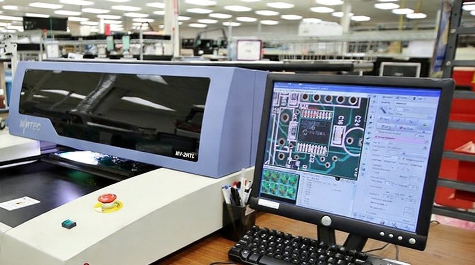
A typical SMT assembly can contain hundreds or even thousands of solder joints. These joints may vary in package size, thermal behavior, pad design, and spacing, but they must still be formed consistently from board to board. This is where the reflow soldering process becomes essential.
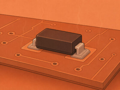
At its core, reflow soldering is the process used to create electrical and mechanical connections between components and the PCB board. It begins after solder paste has been printed onto the PCB pads and components have been placed onto the paste deposits. The assembly then passes through a controlled thermal cycle inside a reflow oven.
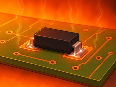
As the temperature rises, the flux within the solder paste becomes active and helps remove surface oxides from the soldering surfaces. The solder alloy then melts, wets the component terminations and PCB pads, and forms the shape of the solder joints. During cooling, the molten solder solidifies into stable joints that secure the components to the board and provide the required electrical connections.
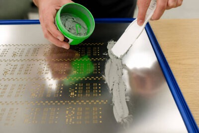
Before the PCB enters the reflow oven, solder paste must first be printed onto the PCB pads through a stainless-steel stencil. Solder paste is a formulated mixture of fine solder alloy particles suspended in a flux medium. The alloy provides the metal that will form the final solder joint, while the flux helps remove surface oxides, promotes wetting, and protects the soldering surfaces during heating.
Many modern electronics manufacturing use lead-free SAC-based solder pastes, such as SAC305 (Sn96.5/Ag3.0/Cu0.5), which has a melting point of around 217°C. Older tin-lead assemblies commonly used Sn63Pb37, a eutectic alloy with a lower melting point of 183°C. This difference is one reason why lead-free reflow profiles generally require higher process temperatures and tighter thermal control.
After solder paste printing, production lines perform SPI (Solder Paste Inspection) to check paste volume, height, area, and positional accuracy. This helps identify printing defects such as insufficient paste, excessive deposits, or stencil misalignment before components are placed.
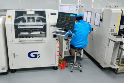
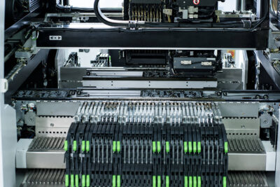
Once the paste has been verified, high-speed pick-and-place machines position surface-mount components onto the solder paste deposits. The tackiness of the solder paste temporarily holds each component in place until the solder melts inside the reflow oven.
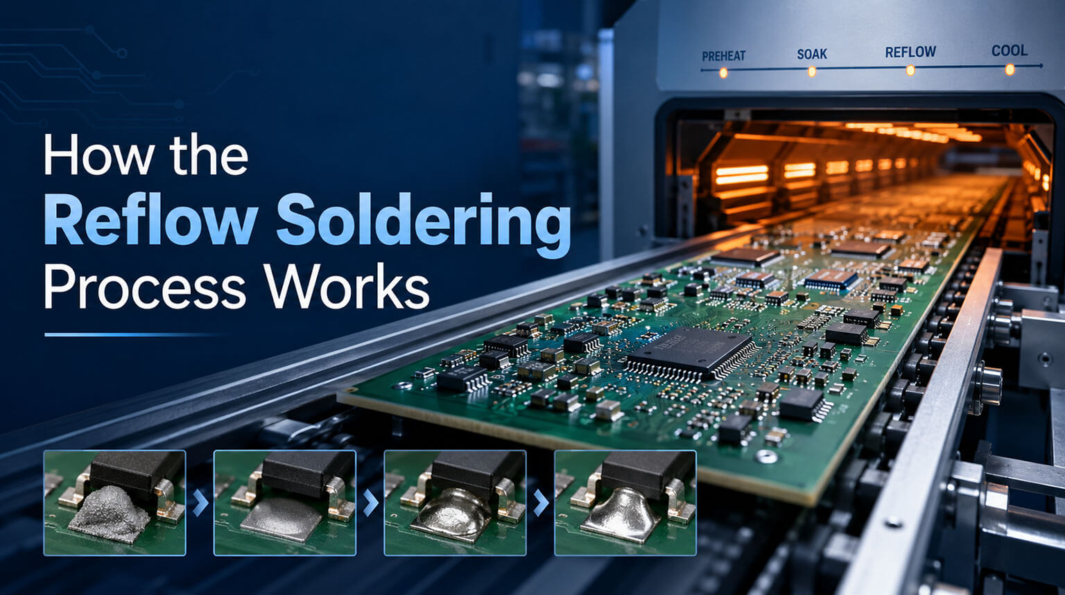
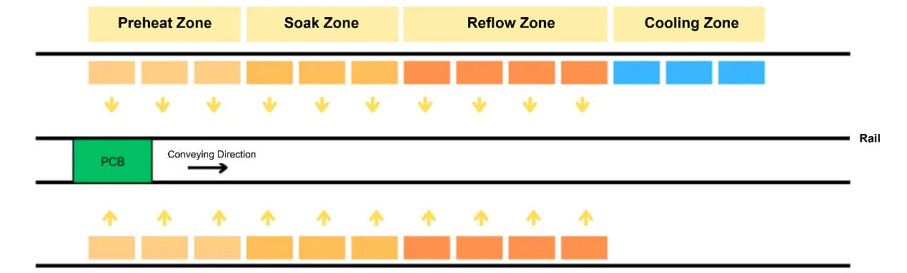
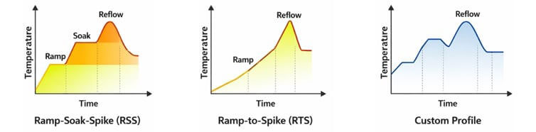
Modern reflow ovens use multiple heating and cooling zones arranged along a conveyor system. As the PCB assembly travels through these zones, the process is commonly described in four stages: preheat, soak, reflow, and cooling, each with its own key parameters.
During preheat, the conveyor brings the board from room temperature up to about 120–150°C. This stage serves several purposes: it gently removes residual solvents from the flux, dries the solder paste, and warms the assembly to reduce thermal shock.
A crucial parameter in this stage is the ramp rate (how fast the temperature rises). Industry guidelines typically call for a gentle ramp of about 1–2°C per second, while in actual production, the ramp is usually kept below about 3°C/s as an upper limit. This rate is controlled with the help of the temperature sensors and control system inside the reflow oven.
The exact preheat ramp depends on board size and mass. For example, for a heavy board with many layers, heating too fast can crack parts; for a light board, a faster preheat may be acceptable.
By the end of preheat, most of the volatile solvents in the flux have boiled off, and the board temperature is fairly uniform.
After preheat, the assembly enters the soak stage, where the board is held at about 150–180°C for roughly 30–90 seconds. At this point, the solder alloy has not yet reached its melting point.
This stage is necessary because a PCB assembly contains materials and components with different thermal behavior. Components connected to large copper pads or metal masses heat more slowly, while small chip components heat faster. Holding the board in this intermediate temperature range gives slower-heating areas time to catch up before the assembly enters the higher-temperature reflow stage, reducing the risk of thermal imbalance and mechanical stress.
During this period, the flux also continues to remove surface oxides and prepare the soldering surfaces for wetting.
Next comes the reflow stage itself, where the board temperature rises above the solder alloy’s melting point, known as the liquidus. For eutectic tin-lead solder, melting occurs at around 183°C, while common lead-free tin-silver-copper alloys, such as SAC305, have a liquidus of around 217–221°C. In a typical SAC305 profile, the peak temperature is often set at about 240°C, roughly 20–30°C above the liquidus. Some profiles may allow peak temperatures up to 250°C, but usually not much higher to avoid component damage.
At this stage, the solder particles in the paste melt and coalesce into fillets. The board temperature typically rises from the end-of-soak temperature up to the peak. The ramp rate here is often on the order of 1–2°C/s. If the ramp is too abrupt, flux gases can boil too quickly and cause solder balls or spattering. If the ramp is too slow, the solder may wet prematurely, causing bridging.
Time Above Liquidus (TAL) is a critical measure that indicates how long the solder stays above its liquidus. Typically, boards are held above the alloy’s melting point for about 30–90 seconds. This ensures the solder has time to fully flow and wet the surfaces. Short TAL, such as under 20 seconds, can result in incomplete wetting. Excessive TAL, especially well over 100 seconds, may expose components to unnecessary thermal stress.
After the peak temperature, the assembly enters the cooling stage, where the molten solder solidifies into final solder joints. Cooling needs to be fast enough to support a fine-grained solder structure, but still controlled enough to avoid thermal shock. In many reflow profiles, the cooling rate is kept at roughly 3–4°C per second.
If cooling is too slow, the solder may form coarser grains, which can reduce joint strength. If cooling is too rapid, the sudden temperature change may introduce stress into the solder joints, components, or PCB materials.
In many reflow ovens, cooling is controlled through dedicated cooling zones or by reducing heat in the final oven sections. Airflow and conveyor speed can also be adjusted to control how quickly the board cools. For example, a cooling zone may be set at around 100°C or lower, allowing the board to cool to below 80°C before it exits the oven. Some production lines also use forced air to increase the cooling rate when needed.
A reflow soldering temperature profile is not a fixed template. It must be adjusted based on the PCB structure, board thickness, layer count, copper weight, component thermal sensitivity, solder paste specification, component distribution, and overall thermal mass.
Most PCBA manufacturers define the profile in terms of several key parameters:
- Ramp to soak: 1–3°C/s
- Soak stage: about 150–200°C for 30–90 seconds
- Ramp to peak: about 1–1.5°C/s
- Peak temperature: about 230–250°C, with around 240°C commonly used for SAC305
- Time above liquidus: about 30–90 seconds
To ensure the profile stays on target, manufacturers use thermal profiling tools on a regular basis. A “golden board” is loaded with multiple thermocouples at key locations (e.g., corner, center, large ICs, etc.). When this board goes through the oven, a profiler records the actual temperature curve for each location. This measured profile is compared against the target. Typically, each zone’s temperature should stay within a small window (for example, ±5–10°C) of its setpoint.
If the profile drifts due to oven lamp aging, belt speed change, or new board designs, the ovens must be re-tuned. For example, if the peak thermocouple shows 5°C low, operators might increase the peak zone setpoint. If ramp rates are off, they might adjust zone spacing or speed.
This feedback loop is essential because reflow soldering must stay within an acceptable process window. Running boards outside that window is not considered acceptable, even if the boards appear to pass electrical testing, because solder joint reliability may still be affected.
Profile data is often tracked statistically using key metrics such as time above liquidus, peak temperature, ramp rates, etc. These values may be plotted in Statistical Process Control (SPC) charts, and any trend out of control limits triggers maintenance. In well-controlled lines, this level of process control is one reason reflow soldering yields can remain very high, often above 99%.
Reflow ovens were once compared mainly by zone count, such as 8-zone, 10-zone, or 12-zone systems. More zones can give the oven finer control over heating and cooling, but zone count alone does not define process capability. In modern SMT production, the more practical question is whether the oven can maintain a stable lead-free profile and, when needed, provide a controlled nitrogen atmosphere.
Lead-free reflow is now the standard process for most RoHS-compliant electronics. The difficulty is not simply switching away from tin-lead solder, but working within a narrower thermal window. Lead-free solder paste needs more heat to wet properly, while laminates, surface finishes, plastic packages, and temperature-sensitive components still have upper temperature limits.
Nitrogen reflow improves the soldering atmosphere rather than the solder alloy or the profile itself. Its main control point is the oxygen level inside the oven, measured in parts per million (ppm). A lower ppm target can suppress oxidation during heating and improve wetting margin. The tradeoff is nitrogen consumption and operating cost, so nitrogen should be selected when it adds real process value.
Even with a well-controlled process, soldering defects can occasionally occur. When they do, the defect often provides useful clues about the underlying process condition.
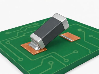
One of the most recognizable defects is tombstoning, where a small chip component lifts from one pad during reflow and stands partially upright. The condition is typically associated with uneven wetting forces caused by thermal imbalance, unequal pad geometry, or inconsistent solder paste deposits.
Solder bridging occurs when unwanted solder connects adjacent pads or component leads. This defect is commonly linked to excessive solder paste, stencil design issues, poor paste release, or component misalignment. Fine-pitch packages are particularly sensitive to bridging.
Another frequently encountered issue is insufficient solder, where the solder volume is inadequate to form a robust joint. Poor stencil transfer efficiency, blocked apertures, or inadequate wetting can contribute to this condition.
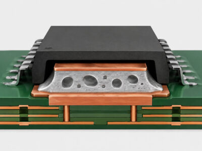
For power devices and components with large thermal pads, voiding may become a concern. Voids are pockets trapped within the solder joint that can affect thermal performance and, in some applications, long-term reliability.
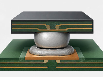
Assemblies containing BGA packages may also experience head-in-pillow defects, where the solder ball and solder paste fail to merge completely during reflow. Factors such as package warpage, oxidation, and improper thermal profiling can contribute to this failure mechanism.
Once the board leaves the reflow oven, the first question is simple: did the solder joints form as intended? AOI is usually the first check because it can quickly catch visible issues such as missing parts, wrong orientation, component shift, lifted leads, solder bridges, and obviously weak joints.
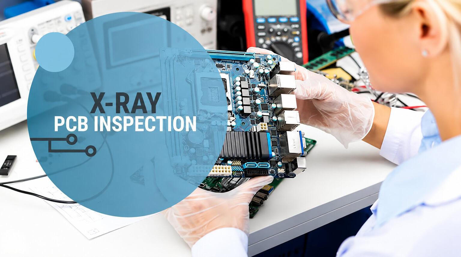
Some joints cannot be judged from the outside. BGA balls, QFN center pads, and large thermal pads often need X-ray review. For products where electrical performance matters, functional testing may also be added after visual or X-ray inspection.
The value of inspection is not only finding bad boards. A repeated bridge may point back to stencil aperture design, paste volume, or placement offset. Voiding may suggest that the profile, thermal pad design, or paste release needs to be reviewed. When inspection results are read this way, they become part of process control rather than just a final gate before shipment.
Successful reflow soldering depends on much more than selecting the right oven settings. Solder paste, stencil design, component placement, thermal profiling, and inspection all contribute to the quality of the final assembly. Small variations at any stage can affect solder joint integrity, manufacturing yield, and long-term reliability.
For this reason, reflow soldering should be managed as part of a complete SMT assembly process, not as an isolated production step.
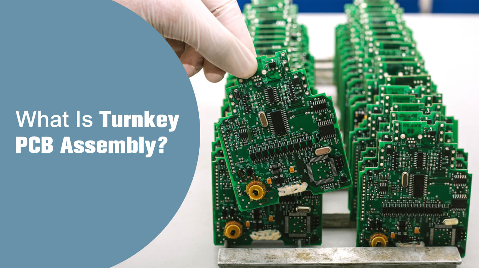
At PCBCool, we provide SMT assembly services for prototypes, small-batch production, and turnkey PCBA projects. Our team supports solder paste inspection, controlled reflow soldering, post-reflow inspection, and testing to help customers turn PCB designs into reliable finished assemblies.