If you’ve ever laid out a board with a fine-pitch BGA and watched your routing space disappear, you already know the problem that via filling is meant to solve. Modern components keep shrinking their pad pitch, while boards are expected to carry more current, handle more heat, and support more routing layers within nearly the same footprint.
Unfilled plated vias can become a problem in these designs. They may wick solder during reflow, create planarity issues under component pads, and take up board space that could otherwise be used for routing.
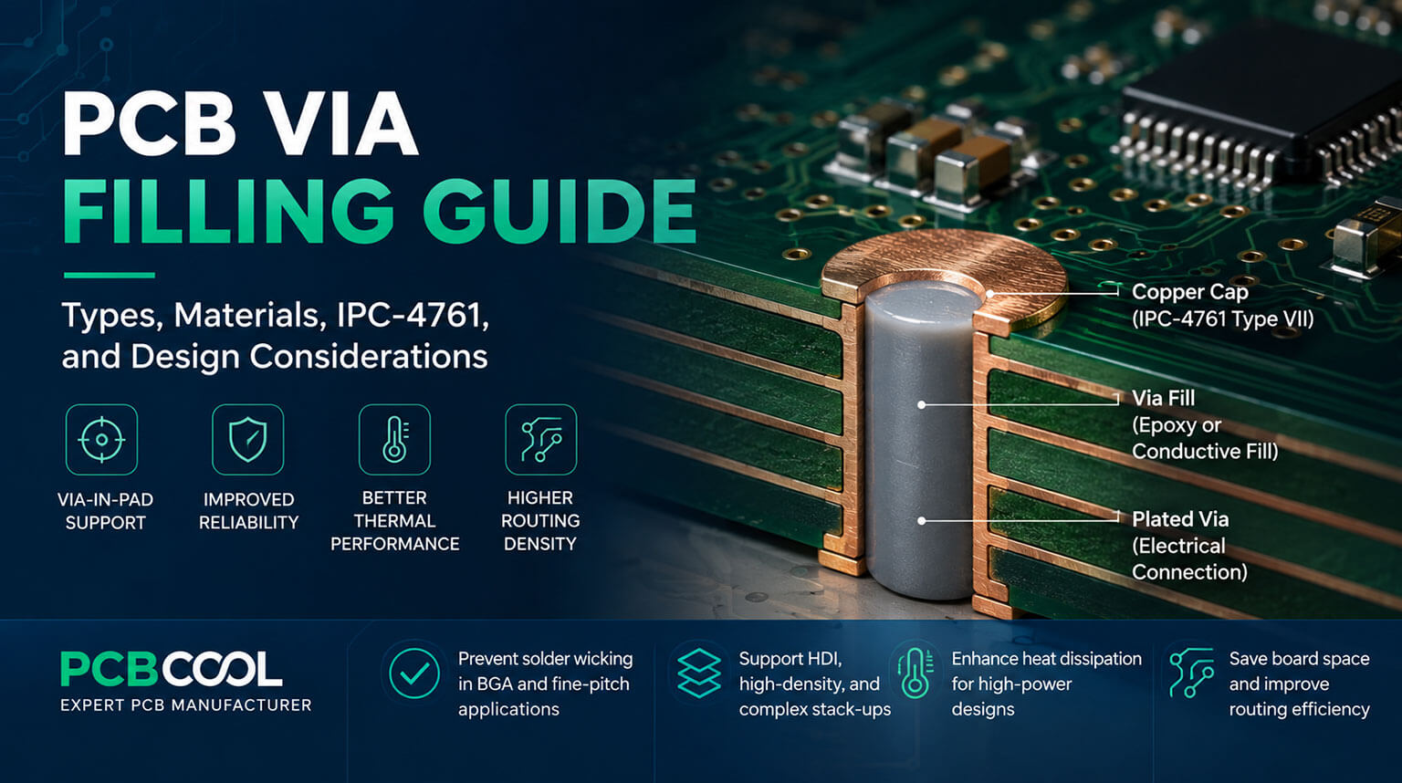
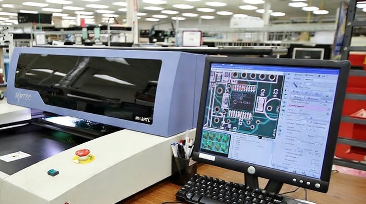
Via filling is used to address these issues. It is the process of filling a drilled and plated via hole with a conductive or non-conductive material to improve reliability, thermal or electrical performance, and overall routing density. It has become standard practice on many high-density PCB designs.
If you’re designing a board with BGAs, fine-pitch components, HDI stack-ups, or high-power circuits, it is worth understanding via filling properly rather than simply specifying “fill all vias” and leaving the decision to the fabricator.
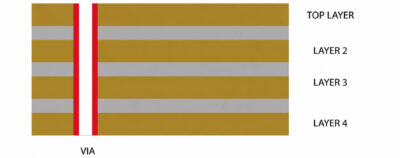
Before getting into via filling, it helps to picture what’s being filled. A via is a plated hole that runs through the board’s layers, electrically connecting copper on one layer to copper on another. In a simple four-layer board, that means a hole drilled straight through the top layer, layer 2, layer 3, and layer 4, with plating along its barrel walls carrying the electrical connection between them.
Left unfilled, that barrel is just open air running through your board. For most components, that’s fine; however, if it is under a BGA pad, it is a liability. Solder during reflow can flow down into the hole instead of staying on the pad, weakening the joint or starving it of solder entirely. The technical term for this is solder wicking, and it is one of the most common root causes of intermittent BGA failures in the field. A joint that looks fine under inspection can still have less solder volume than it needs, simply because some of it disappeared down a via during reflow.
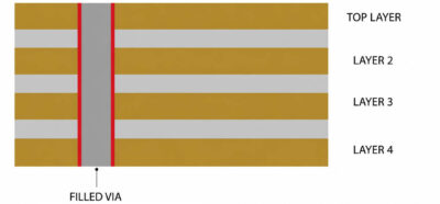
This is also where the line between “drilling a via” and “filling a via” really matters. Drilling and plating give you the electrical connection between layers. Filling is a separate, additional process applied after plating, where a material is deposited into the now-plated barrel to eliminate the open cavity entirely. The two are often discussed together, but they’re distinct manufacturing steps with separate cost lines on a fabrication quote.
Filling that hole with material solves several problems at once, which is why the technique has become close to mandatory on dense modern designs:
- Via-in-Pad (VIP) support — Filling allows you to place a via directly underneath a component pad, including BGA balls, without the solder-wicking problem mentioned above. This alone is often the deciding factor.
- Better thermal dissipation — Particularly true when using conductive fill materials, which give heat a low-resistance path through the board instead of trapping it in an air-filled cavity.
- Improved signal integrity — Filled vias, especially when capped, reduce inductance and improve performance for high-speed signal paths.
- Higher routing density — Because vias can now sit under pads instead of beside them, you free up real estate for escape routing under dense packages.
- Stronger mechanical strength — A filled and capped via creates a flat, solid surface, which matters for reliable SMT assembly.
- Prevention of outgassing — Open via barrels can trap flux residue or air that outgasses during reflow, contributing to solder voids. Filling removes that cavity.
- Reduced layer count — On complex HDI boards, via-in-pad capability can eliminate the need for extra routing layers that would otherwise be required to avoid placing vias under components.
In practice, this shows up most often on:
- Fine-pitch BGAs (0.8 mm pitch or smaller)
- High-power components that need dedicated thermal vias
- HDI and stacked-via designs
- Applications requiring long-term durability
There are two broad categories of via fill, plus a few variations that map onto the IPC-4761 standard. Choosing between them comes down to whether you need the via to actually conduct electricity and heat, or whether you just need it structurally sound and flat.
This is the most cost-effective method and, consequently, the default choice for most via-in-pad applications. The via is filled with an epoxy resin or another non-conductive polymer.
What it does well:
- Provides structural support and a flat, planar surface
- Solves the general via-in-pad problem and prevents solder wicking
- Adds mechanical strength to the board at a low relative cost
What it doesn’t do:
- The fill material is there to plug the hole, not to carry current or heat.
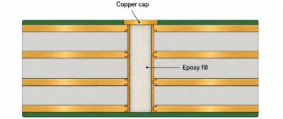
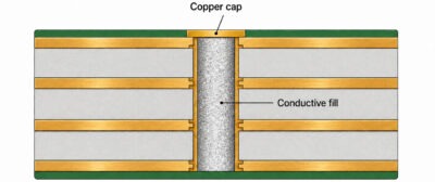
Non-conductive fill is typically followed by copper capping, plating a thin copper layer over the now-flat filled via to produce a solderable surface that behaves just like the rest of the pad.
When you need the via to do more than just stay out of the way, conductive fill is the next step up. Here, the via is filled with conductive epoxy (typically silver- or copper-filled) or with electroplated copper. This category is built for:
- High-current paths, where the via itself needs to carry meaningful current
- Thermal management, where the fill material needs to move heat efficiently away from a hot component
- High-speed signal paths, where electrical continuity through the fill matters for performance
Conductive fill costs more than non-conductive epoxy, but it earns that cost back in applications where the via is doing real electrical or thermal work, not just sitting under a pad.
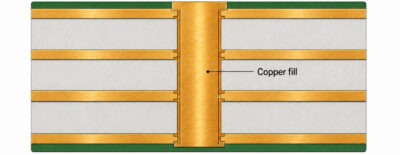
At the top end of the spectrum, vias can be filled with electroplated copper rather than epoxy of any kind. This is sometimes called “copper-plated shut.”
This approach delivers the best conductivity and thermal performance of any via fill method, full stop. It is also the most expensive, both because of the plating process involved and the tighter process control needed to fill a via completely with copper rather than with a resin.
It is reserved for designs where thermal or electrical performance through the via is critical enough to justify the cost, dense power planes, high-current thermal vias under power components, and similar demanding use cases.
If you talk to a fabricator about via fill, they’ll likely reference IPC-4761, the industry standard that defines via protection types. It covers more ground than just filling, but three types are directly relevant here:
- Type V — Filled: The via is fully plugged with material, typically epoxy. Nothing further is done to the surface.
- Type VI — Filled and Covered: The via is filled, then covered with a solder mask on top.
- Type VII — Filled and Capped: The via is filled and then capped with a plated copper layer on the surface, creating a smooth, flat, solid copper pad directly over the via.
Type VII is the one you’ll encounter most often on modern designs, and for good reason. It’s commonly referred to as VIPPO (Via In Pad Plated Over) and it is the configuration that makes true via-in-pad layouts possible. By filling the via and then plating a flat copper cap over it, VIPPO prevents solder from wicking down into the via during assembly, allows the via to sit directly beneath a component pad without compromising the solder joint, and delivers strong electrical and thermal performance on top of that.
For most modern designs using BGAs or fine-pitch components, Type VII is the recommended starting point unless there’s a specific reason, usually cost, to step down to Type V or VI.
Specifying via filling correctly involves more than picking a material. A few design-stage decisions determine whether your fill strategy actually works in fabrication and assembly:
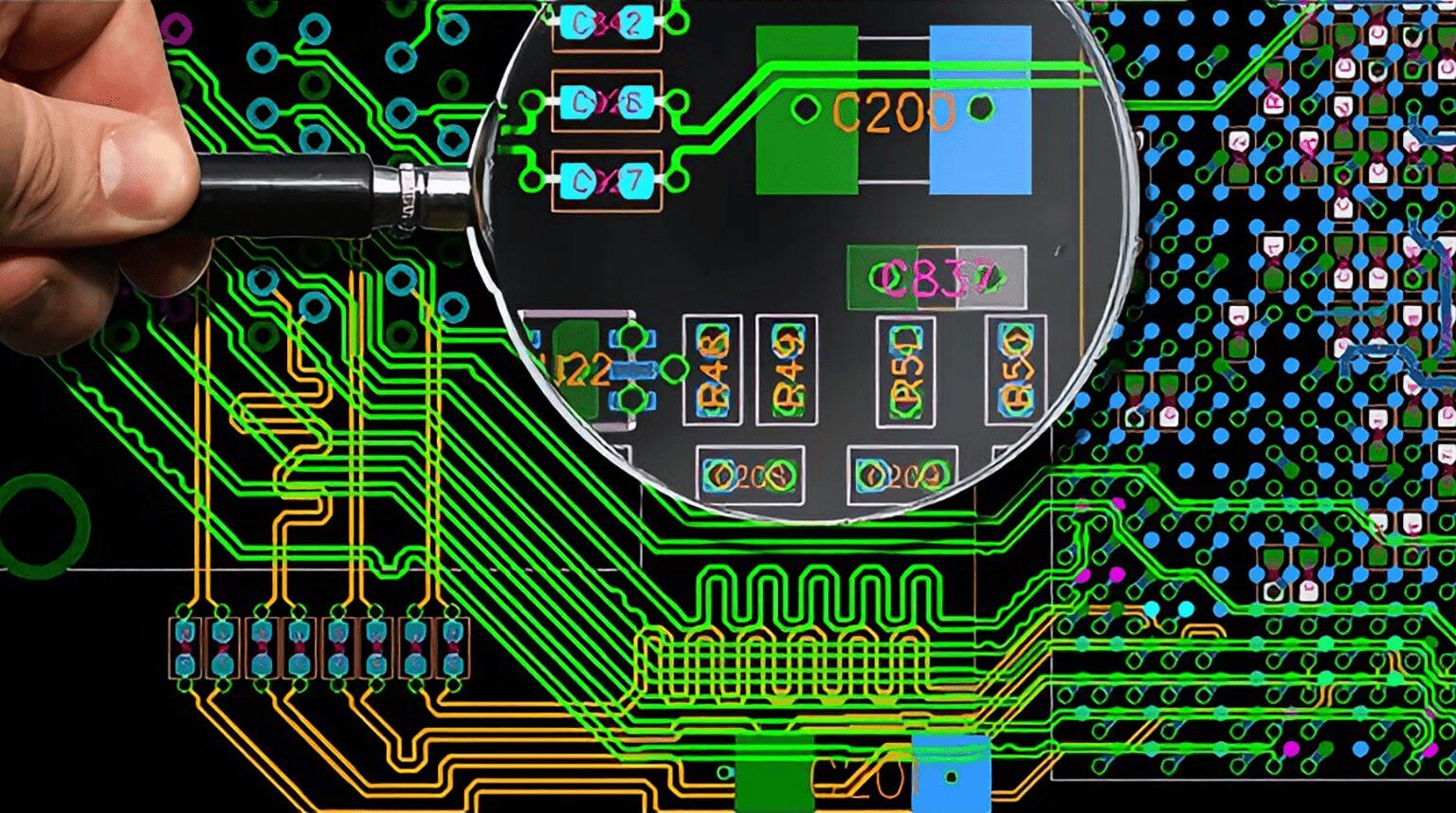
- Via-in-Pad (VIP): When you place a via directly inside a component pad, most commonly under a BGA ball, it must be filled and capped to create a flat, solderable surface. An unfilled or uncapped via-in-pad will cause solder defects during reflow.
- Dogbone vs. Via-in-Pad: A dogbone routing pattern keeps the via off to the side of the pad, connected by a short trace, which avoids the need for filling but consumes extra board space. Via-in-pad saves that space but requires filling and capping to work properly. Which one you choose is largely a function of how tight your pitch and routing constraints are.
- Aspect Ratio: The ratio of via depth to via diameter has a direct impact on how reliably it can be filled. Keep the aspect ratio within reasonable bounds. Your fabricator can advise on their specific process limits to avoid voids or incomplete fill inside the barrel.
- Thermal Relief: For vias placed under BGAs or power components specifically for heat dissipation, use conductive fill rather than standard non-conductive epoxy. Non-conductive fill won’t move heat the way these applications need.
- Fabrication Notes: This is where a lot of via-filling problems actually originate not in the design itself, but in unclear fab drawings. Make sure your documentation explicitly specifies:
- Which vias under BGA pads must be filled and copper-capped (IPC-4761 Type VII)
- The fill material to use (non-conductive epoxy unless otherwise specified)
- Exactly which vias need filling — not every via on the board requires it, and over-specifying drives up cost unnecessarily
That last point is worth repeating on its own: not every via needs filling. Only vias that sit under pads, serve a thermal-critical function, or live in genuinely high-density areas justify the added process step. Filling vias indiscriminately is one of the most common ways designers inflate fabrication costs without any corresponding benefit.
If you are not sure whether your PCB design really needs via filling, PCBCool can help review it before fabrication. We have strong experience with PCB projects involving BGAs, HDI, via-in-pad designs, and filled via requirements.
Once you submit your files, our engineering team will review the design, evaluate whether via filling is necessary, and suggest a practical manufacturing approach based on cost, reliability, and assembly requirements.