As digital systems continue to operate at higher speeds and lower voltage margins, signal integrity (SI) has shifted from a specialized concern to a core design constraint. Issues such as ringing, crosstalk, reflections, and ground bounce are no longer confined to high-end servers or RF systems—they routinely appear in consumer electronics, industrial controllers, and embedded platforms.
Despite the recognition of the above challenges associated with the Signal Integrity of PCBs during the PCB design process, signal integrity problems remain some of the major concerns that are handled during the post-layout process. The fact is that signal integrity failures are not mainly due to a single error but the collective design decisions. Much like PCB cost or manufacturability, signal integrity is largely determined long before the first prototype is built.
This article approaches signal integrity from a design-and-manufacturing-first perspective. Rather than emphasizing simulation analysis based on simulation theory, this pertains to practical PCB design decisions that impact real-world signal characteristics.
Rather than avoiding possible signal integrity effects, signal integrity is minimized so that PCBs operate within a predictable range. This ensures that signal integrity issues are reduced from being a problem.
Signal integrity refers to the ability of an electrical signal to travel from a transmitter to a receiver without excessive distortion, timing uncertainty, or noise. At low speeds, PCB traces behave like simple connections. As edge rates increase, those same traces behave like transmission lines with distributed resistance, capacitance, and inductance.
From a system perspective, signal integrity is affected by:
- Stackup and reference plane continuity
- Trace geometry and routing topology
- Return to current paths
- Through structures and discontinuities
- Power Distribution Stability
Each of these is directly influenced by design decisions in PCB. Poor SI performance is rarely the result of a single “bad trace”; it is usually the consequence of inconsistent design intent across the board.
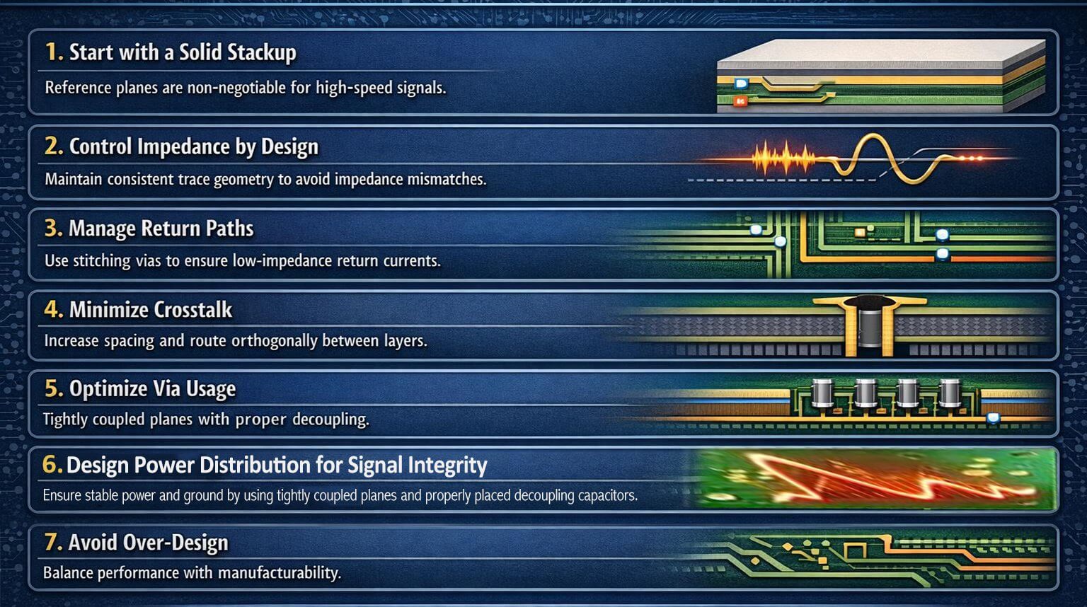
High-speed signals require a continuous, low impedance return path. This return path is almost always provided by a solid ground or power plane adjacent to the signal layer.
From a signal integrity standpoint:
- A signal layer without a solid reference plane is a guaranteed source of noise and EMI
- Splits, voids, or poorly stitched planes force return currents to detour, increasing loop area and radiation
- Consistent plane adjacency minimizes impedance variation and timing uncertainty
A common design mistake is treating the stackups as a mechanical constraint rather than an electrical structure. Signal layers should be intentionally paired with reference planes, not placed arbitrarily to simplify routing.
Trace impedance is heavily influenced by the dielectric thickness between the signal layer and its reference plane. Tight impedance control is impossible if this spacing is undefined or left to the fabricator’s discretion.
Standard dielectric thicknesses improve yield and reduce PCB costs. From an SI perspective, predictable spacing enables accurate impedance calculation and reduces the risk of reflections. Early stackups definition is therefore one of the most powerful tools for reducing signal integrity problems.
When a signal encounters a change in impedance—at a connector, via, or trace width transition—part of the signal reflects toward the source. These reflections manifest as ringing, overshoot, or undershoot, which can violate logic thresholds and timing margins.
Impedance mismatches are rarely dramatic in isolation. The problem arises when multiple small discontinuities accumulate across the signal path.
Maintaining consistent trace width, spacing, and reference plane relationships is essential for impedance stability. Sudden neck-downs, unnecessary width changes, or routing through regions with different dielectric thickness introduce localized impedance steps.
Designers should treat impedance-controlled traces as continuous transmission structures, not flexible routing paths. Minor routing convenience often translates directly into degraded signal quality.
Every signal current is accompanied by a return current. At high frequencies, return current follows the path of least inductance, not least resistance. This almost always means flowing directly under the signal trace in the adjacent reference plane.
When the reference plane is interrupted—by a split, cutout, or layer transition—the return current is forced to spread or detour. This increases loop area, which in turn increases noise, crosstalk, and EMI.
Whenever a signal changes layers, its return current must also transition between reference planes. Stitching vias placed near signal vias provide a low-impedance path for this transition.
From an SI standpoint, missing stitching vias are a frequent and underappreciated source of noise and radiation. From a manufacturing standpoint, adding a small number of stitching vias has negligible cost impact compared to the risk of functional failure.
Crosstalk results from electromagnetic coupling between adjacent signal traces.
It increases with:
- Closer trace spacing
- Longer parallel run lengths
- Faster edge rates
Crosstalk is not purely a spacing issue—it is also a layer planning problem.
Routing adjacent signal layers orthogonally (for example, horizontal on one layer, vertical on the next) significantly reduces broadside coupling.
This is a simple layout discipline that delivers substantial SI benefits with no cost penalty
Not all signals require the same level of isolation. High-speed clocks, differential pairs, and sensitive analog signals should be given priority spacing and routing control.
Applying uniform rules across all nets often leads to unnecessary congestion without meaningful SI improvement.
Every via introduces parasitic capacitance and inductance. At low speeds, these effects are negligible. At high speeds, they can distort signals and create impedance discontinuities.
Key contributors include:
- Via barrel length
- Unused via stubs
- Reference plane transitions
Via stubs act as resonant structures that can severely degrade signal quality. Back drilling or blind/buried vias are effective mitigation techniques, but they add manufacturing cost.
A cost-efficient alternative is thoughtful layer assignment—placing high-speed signals on layers that minimize via depth. Reducing stubs through design is almost always cheaper than removing them through fabrication processes.
Unstable power delivery manifests as ground bounce, jitter, and timing errors. High-speed signals draw transient currents that must be supplied locally and quickly.
From a PCB design perspective:
- Decoupling capacitors must be placed close to load pins, not merely present
- Power and ground planes should be tightly coupled to reduce loop inductance
- Excessive plane segmentation increases impedance and noise
Poor power distribution design often masquerades as a signal integrity problem. In practice, many SI issues are resolved by improving power integrity rather than modifying signal routing.
It is tempting to apply aggressive constraints universally: ultra-wide spacing, extreme impedance tolerances, excessive layer count.
While well-intentioned, this approach often introduces new challenges:
- Increased routing congestion
- Additional layers and costs
- More vias and discontinuities
Effective signal integrity design is targeted and intentional. Constraints should be applied where they matter most, not indiscriminately.
Very tight tolerances add to the fabrication difficulties and minimize yields on the wafers.
The strongest designs have been those that have succeeded in reaching electric specifications with results well within possible manufacturing tolerances.
The issue of signal integrity in PCB design cannot be solved by attempting to eliminate every measurable artifact. It is about creating a stable and predictable electrical environment in which signals behave consistently across temperature, process variation, and production volume.
The most effective signal integrity improvements occur early—during stackup definition, component placement, and routing strategy. Once a board reaches the prototyping stage, available options become limited, expensive, and often reactive rather than corrective.
For hardware teams, the real objective should be clarity of intent: identifying the signals that matter most, understanding the constraints that govern them, and recognizing how early design choices impact both electrical performance and manufacturability.
At PCBCool, we approach signal integrity from this early-stage, manufacturing-aware perspective. As an EMS provider focused on PCB fabrication and assembly, we work with customers before layout decisions are locked in. Our in-house engineering team supports design review, stackup planning, and manufacturability analysis, helping identify potential signal integrity risks at the starting point—where they are easiest and most cost-effective to address.