Designing a printed circuit board (PCB) starts long before routing a single copper trace. It begins with the schematic—the logical blueprint of your electronic system.
A well-crafted PCB schematic does more than define connections; it conveys design intent, enables efficient debugging, and supports a smooth transition to manufacturing.
This guide goes beyond basic schematic drawing, covering the engineering practices, documentation standards, and verification steps needed to create professional-grade schematics that manufacturers can trust.
A PCB board schematic is the logical definition of an electronic system. It specifies how components are electrically connected, how signals flow, and how power is distributed—without describing physical placement or board geometry.
In a hobby project, a messy schematic is an inconvenience. In a production environment, it is a liability. A manufacturing-ready schematic directly impacts:
Clear signal naming and logical grouping reveal mistakes early—such as reversed TX/RX lines, missing pull-ups, or incorrect power connections—before they result in costly PCB respins.
A well-structured schematic drives an accurate Bill of Materials (BOM), helping the factory source the correct parts, footprints, and variants without assumptions.
- Enable Cross-Team Collaboration
Engineers, layout designers, and manufacturing partners must be able to understand the design without tracing “spaghetti wiring” or guessing intent.
- Support Debug & Failure Analysis
When a board fails in the lab or in the field, the schematic is the primary reference for root-cause analysis. Poor organization slows diagnosis and increases downtime.
It is common to confuse schematics with PCB layout. Ambiguity in the schematic creates downstream risks. Here is a simple distinction:
- Schematic: Defines electrical intent—signal relationships, power domains, reference designators, component values, and design constraints.
- Layout: Translates that intent into physical reality—component placement, trace routing, impedance control, creepage, clearance, and thermal behavior.
For a more detailed comparison, see our feature article: Schematic vs. Layout.
Next, we’ll cover the documentation standards and planning required to make your schematic truly manufacturing-ready.
Professional schematic design starts before the first symbol is placed. Documentation standards define how your schematic will be read, reviewed, manufactured, and maintained. These “canvas rules” must be established upfront.
Choose a page size that supports readability and logical density. Avoid forcing a complex CPU or SoC design onto a single small sheet.
| Page Size | Typical Usage |
|---|
| A4 / Letter | Simple breakout boards or small sub-circuits |
| A3 / Tabloid | Industry standard; balanced density and readability for screen review and printing |
| A2 / C | Very complex systems or backplanes (use sparingly; difficult to print and review) |
A schematic that cannot be comfortably reviewed on-screen or printed for discussion slows design reviews and increases interpretation errors.
Never leave schematic pages labeled as “Sheet1” or “Sheet2”. Page names should communicate function and system context.
Recommended Structure:
Example: PWR_01 (Power), MCU_01 (Processing), IO_02 (Interfaces)
- Logical Grouping
- Group A: Power Entry & Regulation
- Group B: Microcontroller & Digital Logic
- Group C: Analog Front End
- Group D: Connectors & I/O
Consistent naming allows layout engineers, manufacturers, and reviewers to navigate the design without reverse-engineering your intent.
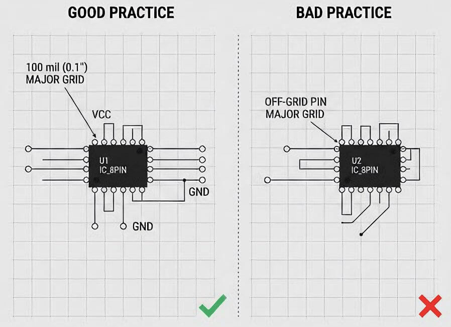
The grid is non-negotiable. Most EDA tools default to a 100 mil (0.1″) grid, and this should remain your primary alignment reference.
Rules:
- Place all component pins on the 100 mil grid
- Use finer grids (50 mil or 25 mil) only for text alignment or label movement
- Never route wires or place pins off-grid
Why this matters:
Off-grid pins create wires that visually appear connected but are electrically open. These errors often survive ERC checks and only surface during layout or bring-up—when fixes are costly.
Every schematic sheet must contain a fully populated title block. In professional environments, this is a revision control and accountability requirement, not decoration.
Mandatory fields:
- Project Name: System or product name
- Sheet Name: Specific function (e.g., “5V Buck Regulator”)
- Revision: Rev 1.0, Rev A, etc.
- Date: Last modification date
- Author: Responsible engineer
Incomplete title blocks break traceability and complicate design audits, especially when multiple revisions circulate.
Reserve a dedicated area—typically the first sheet—for Electrical Notes.
Common examples include:
- Default assembly assumptions
“All resistors are 1% 0603 unless otherwise specified.”
“R40 populated = Boot from Flash.”
Maintain a revision table on the first page to record what changed, who changed it, and when. This is critical for long-term support, ECOs, and manufacturing continuity.
Do not begin by placing random components. Start with structure.
Block Diagram Creation
Create a high-level block diagram that defines the major functional modules.
Typical flow:
Power → Processing → Interfaces
This step helps estimate schematic complexity, page count, and hierarchy before detailed design begins.
Schematic readability relies on consistent visual logic. Follow standard western reading conventions:
- Inputs: Left
- Outputs: Right
- Power: Top
- Ground: Bottom
Breaking these conventions forces readers to mentally “decode” signal flow and increases review time.
For designs exceeding five pages, hierarchical schematics are strongly recommended.
- Top Sheet: Functional blocks representing sub-systems
- Child Sheets: Detailed circuitry
Benefits:
- Clear system overview
- Faster navigation during reviews
- Reusable modules (e.g., duplicating a motor driver block without redrawing)
Hierarchical structure scales better as designs evolve from prototype to production.
Choose an EDA (Electronic Design Automation) tool that fits your workflow and project complexity:
- KiCad: A free, open-source option with increasing industry adoption; suitable for startups and small teams.
- Altium Designer: The corporate standard for high-speed, multi-layer, and complex PCB designs.
- OrCAD / Eagle: Legacy tools still widely used in certain industries or for maintaining older projects.
Before placing any components, organize your project files to streamline collaboration and future maintenance. A recommended folder structure:
/Datasheets → Store all component datasheets locally
/Libraries → Project-specific symbols and footprints
/Output → Gerbers, BOMs, PDFs, and other manufacturing outputs
Correct symbols and libraries are critical to avoid schematic errors and downstream manufacturing issues.
- Standard Reference Designators: Maintain consistency to ensure the assembly house can locate components efficiently.
| Designator |
Component Type |
| R |
Resistor |
| C |
Capacitor |
| L |
Inductor |
| D |
Diode / LED |
| Q |
Transistor (BJT, FET) |
| U |
Integrated Circuit (IC) |
| J / P |
Connector / Header |
| TP |
Test Point |
- Use Standard Libraries: Avoid creating custom symbols unless necessary.
- Manufacturer Parts: Preferred; these often link directly to verified footprints.
- Generic Parts: Acceptable for basic components like resistors or capacitors, but always verify the footprint matches the intended package.
- Heterogeneous Symbols: For large ICs (FPGAs, MCUs), split symbols into multiple functional blocks (e.g., Part A: Power, Part B: GPIO, Part C: USB) to maintain schematic readability and reduce clutter.
Begin your schematic with the power supply—without stable power, the rest of the circuit won’t function correctly.
- Define Inputs: USB, battery, or DC jack.
- Add Protection: Include fuses, TVS diodes, or other overvoltage protection devices.
- Add Regulation: Specify voltage regulators such as LDOs or buck converters.
Tip: Keep the power section clear and logically structured; it serves as the foundation for the entire schematic.
Organize your schematic by functional modules:
- Place the MCU or processor centrally on its sheet.
- Group decoupling capacitors immediately next to the power pins they support.
- Place related peripherals nearby to maintain clear signal flow.
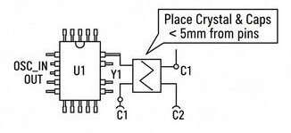
Clock circuitry is highly sensitive; proper placement is essential for signal integrity.
- Position the crystal symbol close to the MCU oscillator pins.
- Add a text note for the layout engineer:
“Place Crystal & Capacitors < 5mm from oscillator pins.”
Avoid routing wires randomly across the page:
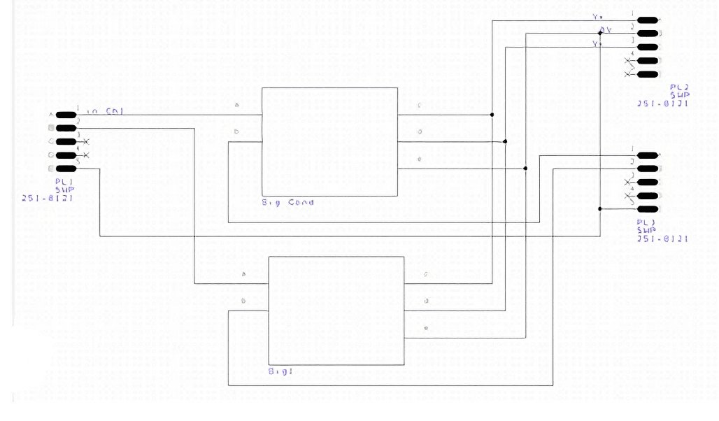
- Long crossing wires create “spaghetti schematics,” which are difficult to debug and error-prone.
- Keep nets organized, and use short, direct connections wherever possible.
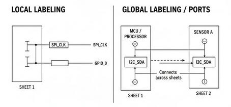
Use labels consistently to simplify multi-sheet schematics:
- Local Labels: Connect signals within the same sheet.
- Global Labels / Ports: Connect signals across sheets.
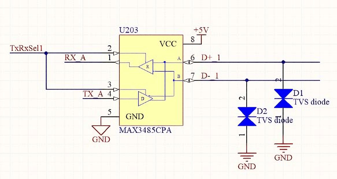
- Descriptive Naming: Use clear, functional names—e.g., I2C_SDA is preferred over generic names like NetC4_2.
Visual hierarchy improves readability:
- Data Buses: Represent grouped signals with thick bus lines (e.g., DATA[0..7]).
- Control Signals: Keep separate from high-speed data paths for clarity.
Tip: Maintain a left-to-right signal flow convention (inputs on the left, outputs on the right) to align with standard engineering practices.
Every EDA tool provides an Electrical Rule Check (ERC) or Design Rule Check (DRC)—use it before finalizing your schematic. These checks catch common errors such as:
- Floating Inputs: Pins that require a connection but are unconnected.
- Short Circuits: Two power nets incorrectly connected (e.g., 3.3V tied to GND).
- Drive Conflicts: Outputs mistakenly connected to other outputs.
ERC/DRC is your first line of defense, but it cannot replace manual verification of logic.
Some errors require a human eye:
- Ensure RX pins connect to TX pins correctly—avoid RX-to-RX or TX-to-TX mistakes.
- Verify decoupling capacitor values against the datasheet.
- Confirm Pin 1 orientation on symbols matches the footprint.
Manual cross-checking prevents functional issues that automated checks may miss.
The Bill of Materials (BOM) is the blueprint for procurement and assembly. Include:
- MPN (Manufacturer Part Number): Unique identifier for each component.
- Value: e.g., 10kΩ, 0.1µF.
- Package: e.g., 0402, 0603, SOIC-8.
- Description: Detailed text for sourcing and assembly teams.
Before handing off to manufacturing, validate the BOM:
- Are there parts labeled TBD or DNI (Do Not Install)?
- Are quantities accurate for each component?
- Are voltage ratings and tolerances sufficient for the design requirements?
Once the schematic is verified and approved:
- Generate the Netlist: A file that defines all electrical connections for the layout tool.
- Assign Footprints: Ensure each symbol is mapped to the correct physical footprint.
- Define Constraints: Specify rules for high-voltage, high-current, or high-speed nets (e.g., “50Ω impedance for USB traces”).
A clear and verified handoff reduces iteration cycles between schematic capture and PCB layout, saving time and preventing costly errors.
- Mirroring Symbols: Avoid mirroring components horizontally without checking pin orientation. Some ICs and connectors may have non-obvious pin ordering, and mirroring can cause functional errors.
- Hidden Pins: Certain symbols hide power or ground pins by default. Always reveal and connect these pins to the appropriate nets to prevent unintentional floating connections.
Professional Tips
Include test point (TP) symbols on all critical power rails and important signal lines. Properly placed test points simplify debugging, signal verification, and manufacturing troubleshooting.
Before releasing your schematic to layout or manufacturing, verify that all critical elements are complete and compliant with professional standards:
| Check Item | Description / Standard |
|---|
| Page Size | Appropriate for design complexity (typically A3 for multi-sheet schematics). |
| Grid | All components aligned to a 100 mil (0.1″) grid to ensure clean connections. |
| Title Block | Fully populated on every sheet with project name, sheet name, revision, date, and author. |
| Reference Designators (RefDes) | Each component has a unique identifier (e.g., R1, R2, C1). |
| Signal Flow | Inputs enter from the left, outputs exit to the right; power flows from top, ground returns to bottom. |
| Decoupling Capacitors | Properly placed adjacent to IC power pins to minimize noise and voltage drops. |
| Electrical Rule Check (ERC) | Run ERC/DRC to confirm the schematic is free of floating pins, shorts, and other electrical errors. |
| BOM Verification | All components include valid Manufacturer Part Numbers (MPNs), values, packages, and descriptions. |
A schematic is far more than a drawing—it is the blueprint for your entire hardware design. A clean, well-documented schematic ensures that your design intent is preserved through layout, manufacturing, and testing. By following these industry-grade standards, you reduce costly board spins, save time and money, and make your design easier for engineers to understand, debug, and maintain.
Once your schematic is complete, partnering with a knowledgeable PCB manufacturer can take your design to the next level. PCBCool does more than just fabricate and assemble boards—they provide end-to-end support to help hardware teams succeed. Our services include:
- Manufacturing & Assembly: High-quality PCB production with fast turnaround times.
- Design Verification Assistance: Review your schematics and BOMs to catch potential issues before production.
- Engineering Support: Guidance on manufacturability, component selection, and layout considerations.
By combining professional schematic practices with PCBCool’s comprehensive services, your designs become truly manufacturing-ready, reliable, and optimized for production, giving you confidence from prototype to full-scale deployment.