In today’s world of autonomous vehicles, industrial automation, and advanced sensing, radar technology has become one of the most critical enablers of perception and safety. From detecting obstacles on the highway to mapping environments for drones, radar systems work reliably in darkness, fog, rain, and dust — conditions where cameras and LiDAR often struggle.
Behind this performance is a highly specialized radar PCB. It is not just a standard PCB used in a radar product, but a board that must support RF transmission, antenna integration, and strict manufacturing control.
If you are working on a radar PCB project, this article can serve as a practical starting point. We will begin with the basic definition of a radar PCB, then move into stackup planning and DFM considerations. If you need it, then let’s get started!
A Radar PCB is a specialized circuit board designed to generate, transmit, receive, and process high-frequency radio frequency (RF) signals used in radar systems. While it may look like a normal circuit board, it is engineered to operate reliably at microwave and millimeter-wave (mmWave) frequencies — typically between 24 GHz, 60 GHz, and 77–81 GHz for modern applications.
At these extremely high frequencies, the PCB no longer behaves like a simple interconnect. Every copper trace acts as a transmission line, and even millimeter-level imperfections can significantly degrade performance. This makes radar PCB design one of the most demanding areas in electronics engineering.
Here is core functions of the radar PCB:
- Signal Generation: Generates the RF signal (continuous wave or pulsed) using a radar transceiver IC.
- Transmission: Amplifies and routes the signal to the transmitting antenna.
- Reception: Captures weak reflected echoes from targets through the receiving antenna.
- Signal Processing: Routes received signals to ADCs and processors (MCU/DSP/SoC) for analysis.
- Power Management & Control: Supplies clean power to sensitive RF components while handling digital interfaces.
To quickly understand why radar PCB are different, we can compare them with conventional PCB from several key design and manufacturing aspects.
FMCW radar transmits a continuous signal whose frequency changes linearly, often called a chirp, and can measure both range and velocity through Doppler analysis. Typical frequencies include 76–81 GHz for automotive radar, 60 GHz for industrial sensing, and 24 GHz for some lower-frequency radar systems.
Key PCB Requirements:
- Excellent phase linearity and stability
- Low phase noise across the chirp bandwidth
- High isolation between Tx and Rx paths
- Precise impedance control for RF traces and antenna feeds
- Stable material performance at microwave or mmWave frequencies
Pulsed radar sends short, high-power RF pulses and measures the time delay of the returned echo. It is a classic radar architecture often used in weather radar, marine radar, and long-range detection systems. Depending on the application, its operating frequency may range from around 10 GHz to much higher microwave or mmWave bands.
Key PCB Requirements:
- High-power handling for RF power amplifier sections
- Fast and stable transmit/receive switching
- Good timing precision with low jitter
- Strong isolation to protect the receiver during transmission
- Reliable thermal design for high-power RF components
CW Doppler radar uses a continuous fixed-frequency signal to detect motion or speed through Doppler frequency shift. It is simpler than FMCW radar and is often used in speed detection, automatic doors, and vital-sign sensing. Because it does not easily measure range without modulation, its PCB design usually focuses more on compact layout, sensitivity, and cost control.
Key PCB Requirements:
- Compact and cost-efficient layout
- Simple but stable RF transmission line routing
- Good receiver sensitivity for weak reflected signals
- Clean power supply for low-noise RF performance
- Proper isolation between transmit and receive paths
Phased array radar uses multiple antenna elements with controlled phase shifts to steer the beam electronically without mechanical movement. It is used in aerospace systems, defense tracking, 5G/6G sensing, and other beam-steering applications. Because many RF channels must work together, PCB layout consistency becomes critical.
Key PCB Requirements:
- Tight phase and amplitude matching between channels
- Multiple identical RF paths with controlled length
- Precise antenna spacing and feed-line geometry
- Complex beamforming network layout
- High layer count and carefully controlled via transitions
MIMO radar uses multiple transmit and receive channels to create a virtual antenna array. This improves angular resolution while keeping the physical antenna size relatively compact. It is commonly used in high-resolution automotive radar, smart sensing, and compact radar modules that need better object separation.
Key PCB Requirements:
- Multiple synchronized Tx/Rx channels
- Excellent channel-to-channel isolation
- Accurate antenna spacing and feed-line length matching
- Stable impedance control across all RF paths
- Careful integration of RF, antenna, and digital signal-processing sections
For radar boards, the key question is not only “which material is better,” but which layers actually need high-frequency material.
For critical RF paths, antenna feed lines, and mmWave signal areas, low-loss materials are usually preferred. Materials such as Rogers RO3003, Rogers RO4350B, Astra MT77, or similar high-frequency laminates can provide more stable dielectric performance than standard FR-4. This is especially important for 24 GHz, 60 GHz, and 77–81 GHz radar designs, where small material variations can shift impedance or antenna behavior.
FR-4 may still be used in digital control, power, or lower-speed routing areas. For this reason, many radar PCB use a hybrid stackup: low-loss material is placed in the RF and antenna layers, while FR-4 is used in less sensitive sections. This helps balance RF performance and manufacturing cost.
When selecting a substrate material, designers should focus on these factors:
- Dk Stability: A stable dielectric constant helps maintain predictable impedance and antenna behavior.
- Df / Loss Tangent: Lower Df reduces signal loss, especially at mmWave frequencies.
- Copper Roughness: Rough copper increases conductor loss and may affect RF performance.
- Thickness Tolerance: Dielectric thickness variation can change impedance and antenna resonance.
- Thermal Stability: The material should remain stable during assembly and operation.
A 4-layer radar PCB is usually used for simpler or lower-frequency radar designs. It can support basic RF routing and antenna integration while keeping cost and manufacturing complexity lower.
A 6-layer stackup is common for more demanding radar modules, especially when the design needs better RF isolation, cleaner reference planes, and separation between RF and digital sections.
An 8-layer stackup is suitable for complex MIMO radar, phased array radar, or compact radar modules with multiple RF channels. It gives designers more space for antenna feeds, RF routing, ground isolation, digital routing, and power distribution.
Impedance control is critical in radar PCB design because RF energy must pass through traces, vias, connectors, and antenna feeds with minimal reflection and loss. For most radar RF paths, the common target is 50Ω single-ended impedance.
A practical impedance control process usually includes:
- Confirm the operating frequency and RF path requirements.
- Select the material and stackup before routing begins.
- Choose the proper transmission line structure, such as microstrip, stripline, CPW, or GCPW.
- Calculate the trace width and spacing based on the final stackup.
- Keep the reference ground plane continuous under RF traces.
- Avoid sudden width changes, unnecessary vias, and uncontrolled stubs.
- Review transitions through pads, vias, connectors, and antenna feeds.
- Use simulation for critical RF paths, especially in mmWave designs.
- Add impedance requirements and test coupons to the fabrication drawing.
For radar PCB, impedance discontinuity often comes from transitions rather than straight traces. Vias, bends, component pads, connector launches, and antenna feeds should be reviewed carefully. In high-frequency designs, 3D EM simulation is often needed to verify these areas before fabrication.
This is the most commonly used structure for radar PCB: Signal trace on the top (or bottom) layer with a ground plane directly below it, separated by dielectric material.
Advantages:
- Easy to fabricate
- Excellent for integrating patch antennas directly on the same layer
- Simple transitions to components
- Lower cost
Disadvantages:
- Higher radiation loss at very high frequencies
- More sensitive to external interference
- Slightly higher loss compared to shielded structures
Application
Antenna feed lines, transmitter output, and outer layer routing.
It is a signal trace embedded between two ground planes (sandwiched in inner layers).
Advantages:
- Excellent shielding and isolation
- Lower radiation and crosstalk
- More consistent impedance
- Better for sensitive receiver signals
Disadvantages:
- Harder to access (requires vias for transitions)
- Not suitable for antenna placement
- Slightly more complex manufacturing
Application
Critical internal RF routing, high-isolation paths, and between Tx/Rx sections.
It is a signal trace with ground planes running on the same layer on both sides of the trace.
Advantages:
- Good isolation and shielding
- Easier component mounting (no vias needed for grounding)
- Flexible impedance control
Disadvantages:
- Requires more board space (ground strips on sides)
- Higher loss if not properly designed
It is a CPW with an additional ground plane on the bottom layer.
Advantages:
- Combines benefits of microstrip and CPW
- Excellent mode suppression
- Very good for high-frequency transitions (to MMIC packages)
- Lower crosstalk and radiation
- Easier via fencing for isolation
Application
77 GHz designs, transitions from IC to transmission line, and high-isolation areas.
Through-hole vias can leave unused barrel sections, known as via stubs. At mmWave frequencies, these stubs may create resonance and signal reflection. This is especially important in 77 GHz radar designs, where the wavelength inside the dielectric is very short.
Common methods for reducing via stubs include:
- Back Drilling: Removes the unused portion of a through-hole via after drilling and plating.
- Blind Vias: Connect an outer layer to an inner layer without passing through the full board.
- Buried Vias: Connect only internal layers.
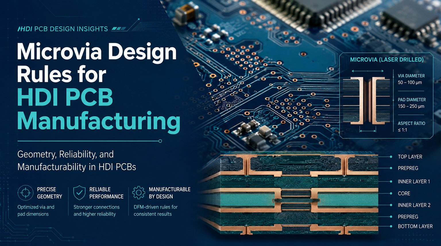
- Microvias: Laser-drilled small vias, often used in dense RF or antenna areas.
Notes: Blind vias and microvias can improve RF transitions, but they also increase fabrication complexity.
A high-frequency via transition should be designed as part of the RF path, not treated as a simple drill hole.
For critical radar paths, designers should:
- Keep the transition as close to 50Ω as possible.
- Use ground vias around the signal via to create a more controlled return path.
- Optimize antipad size instead of using default clearance values.
- Avoid unnecessary layer changes in RF routes.
- Use trace-width compensation near the via when needed.
- Check critical transitions with 3D EM simulation.
Via fencing is commonly used around RF traces, especially for microstrip and GCPW structures. Ground vias placed along both sides of the RF path help suppress unwanted modes and improve isolation between Tx and Rx sections.
For 77 GHz radar designs, ground via spacing is often kept very tight, commonly around 0.5 mm to 1 mm, or based on a rule such as λ/10 to λ/20 using the effective wavelength in the PCB structure.
The ground vias should be connected to continuous reference planes. If the ground structure is broken or too far from the RF trace, via fencing will not provide the expected isolation.
The following are the key design considerations:
Placement:
- Place antenna arrays near the edge or corner of the PCB for better radiation clearance.
- Keep a sufficient ground plane around the patches (typically λ/4 or more).
- Avoid placing components, connectors, or shielding cans near the antennas.
- Maintain clearance from board edges (usually 5–10 mm depending on frequency).
Patch Dimensions & Tolerances:
- At 77 GHz, patch size is very small (~1–2 mm).
- Manufacturing tolerance should be ±0.05 mm or better.
- Even 0.1 mm error can shift resonance frequency significantly.
Feed Line Design:
- Use short, well-matched 50 Ω transmission lines (Microstrip or GCPW).
- Minimize bends and vias in the feed network.
- Ensure excellent phase and amplitude matching across all elements in an array.
Stackup Influence:
- Antenna performance is highly dependent on the dielectric thickness and Dk of the top layers.
- Rogers RO3003 or similar low-loss materials are preferred for the top RF layers.
Mutual Coupling & Isolation:
- Maintain proper spacing between Tx and Rx antenna arrays.
- Use via fences, guard traces, or metal shielding for better isolation.
In radar PCB projects, small design choices often decide the final result. A board may look correct in layout software, but its real performance depends on whether the design can be manufactured with stable materials, accurate tolerances, and repeatable process control.
That is why radar PCB manufacturing should not wait until the final Gerber release. Early review can help identify risks before they become prototype failures or costly redesigns.
PCBCool helps customers turn radar PCB designs into manufacturable boards. Whether your project is still in the design stage or ready for fabrication, our engineering team can review your files, check key manufacturing risks, and support reliable production.
Send your project details to PCBCool, and we will help you move from radar PCB design to a board that can actually be built and tested.