
Blog
What Is Vacuum Etching in PCB Manufacturing
Electronic devices are becoming smaller, while the circuits inside them continue to carry more functions. To support higher routing density in limited board space, many designs now rely on HDI, microvias, dense BGA fanout, and fine trace/space rules.
However, building an advanced PCB is not only about drilling smaller holes or adding more layers. When the trace and space reach 3/3 mil, the real challenge is whether the copper pattern can be formed cleanly, evenly, and repeatedly.
This is where vacuum etching becomes important. For demanding fine-line boards, PCBCool may use vacuum-assisted etching to improve etching uniformity and support more stable line-width control.
What Is Vacuum Etching in PCB Manufacturing
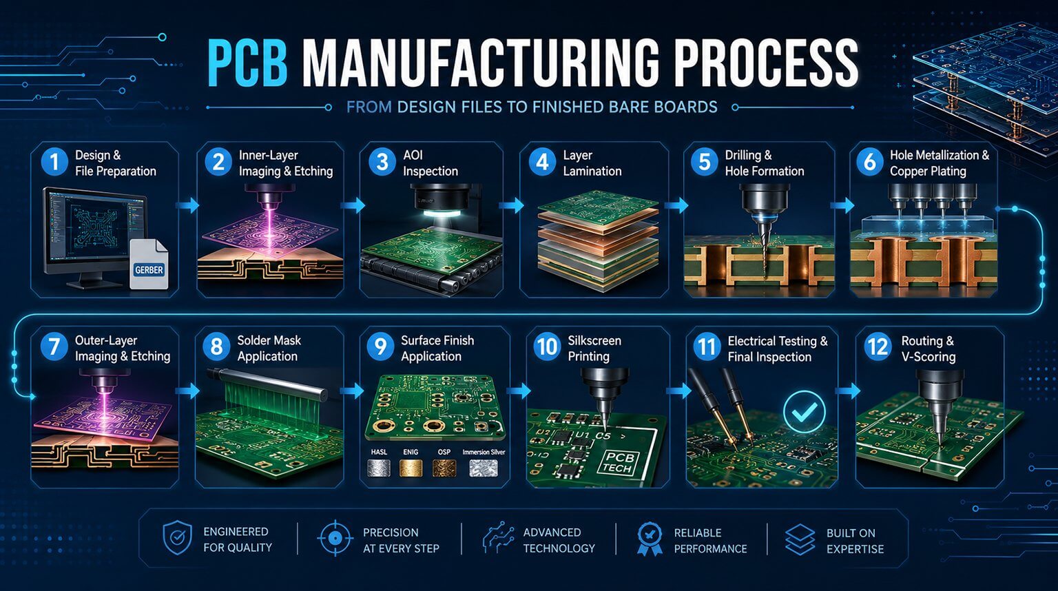
PCB etching is the process of removing unwanted copper from a copper-clad laminate to form the final circuit pattern. After imaging and developing, the areas that must remain as copper traces are protected by photoresist, while the exposed copper is removed by a chemical etching solution.
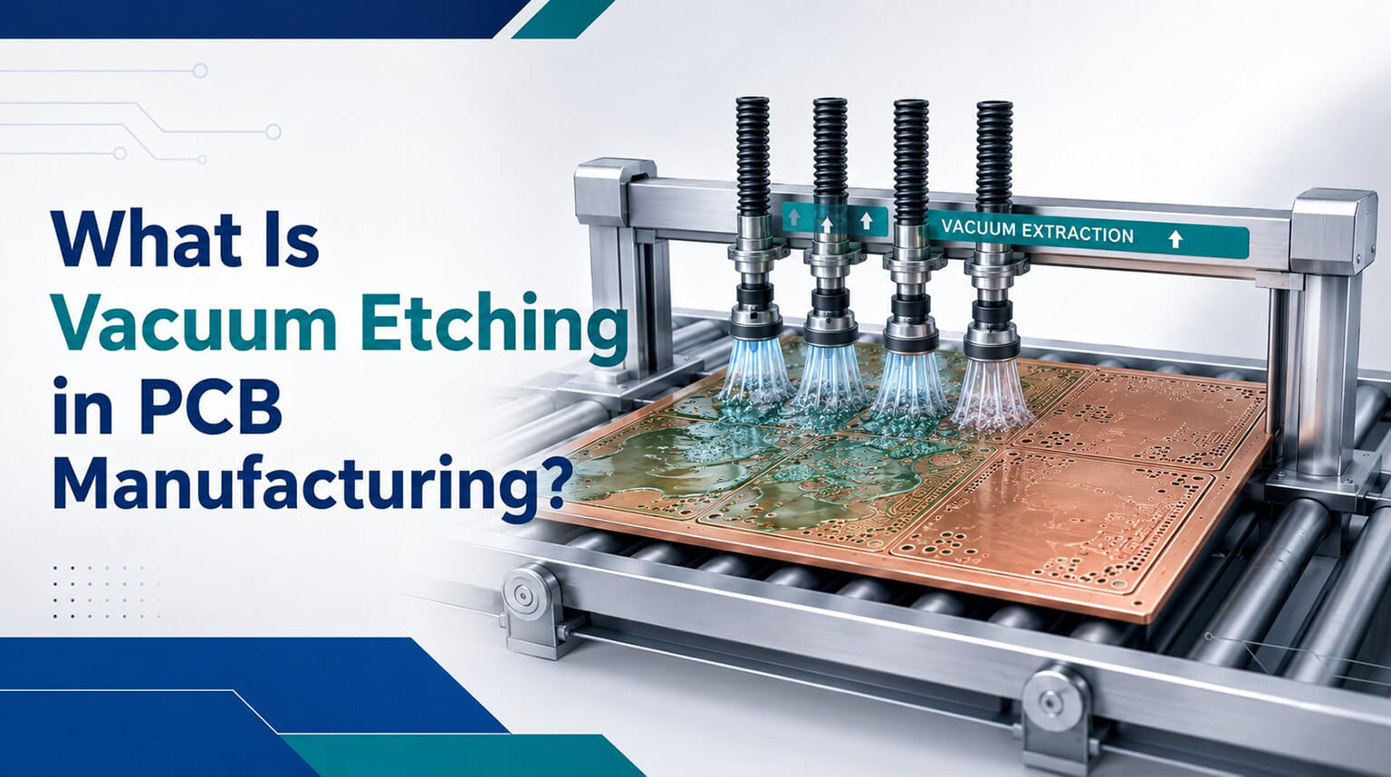
Traditional wet etching uses sprayed etchant to react with and remove the exposed copper. Vacuum etching follows the same basic wet etching principle, but adds a suction or extraction system to remove spent etchant from the board surface more actively.
In practical terms, vacuum etching is not a completely different etching method. It is a more controlled version of wet etching. By improving etchant exchange, it helps fresh solution reach the copper surface more consistently, which is especially valuable for fine-line PCB production.
Vacuum Etching vs. Standard PCB Etching
| Item | Standard PCB Etching | Vacuum-Assisted Etching |
|---|---|---|
| Etchant Removal | Mainly depends on spray flow and gravity | Uses suction to remove spent etchant more actively |
| Etchant Exchange | May be less uniform in difficult areas | Helps fresh etchant reach the copper surface faster |
| Puddle Effect | More likely on the top side of horizontal panels | Helps reduce surface accumulation of spent etchant |
| Fine-Line Control | More difficult near process limits | Better suited for demanding trace/space requirements |
| HDI PCB Suitability | Suitable for many standard PCB | More useful for fine-line and HDI PCB manufacturing |
| Main Value | General copper removal | Improved etching uniformity and line-width control |
Why 3/3 Mil Makes Etching More Difficult
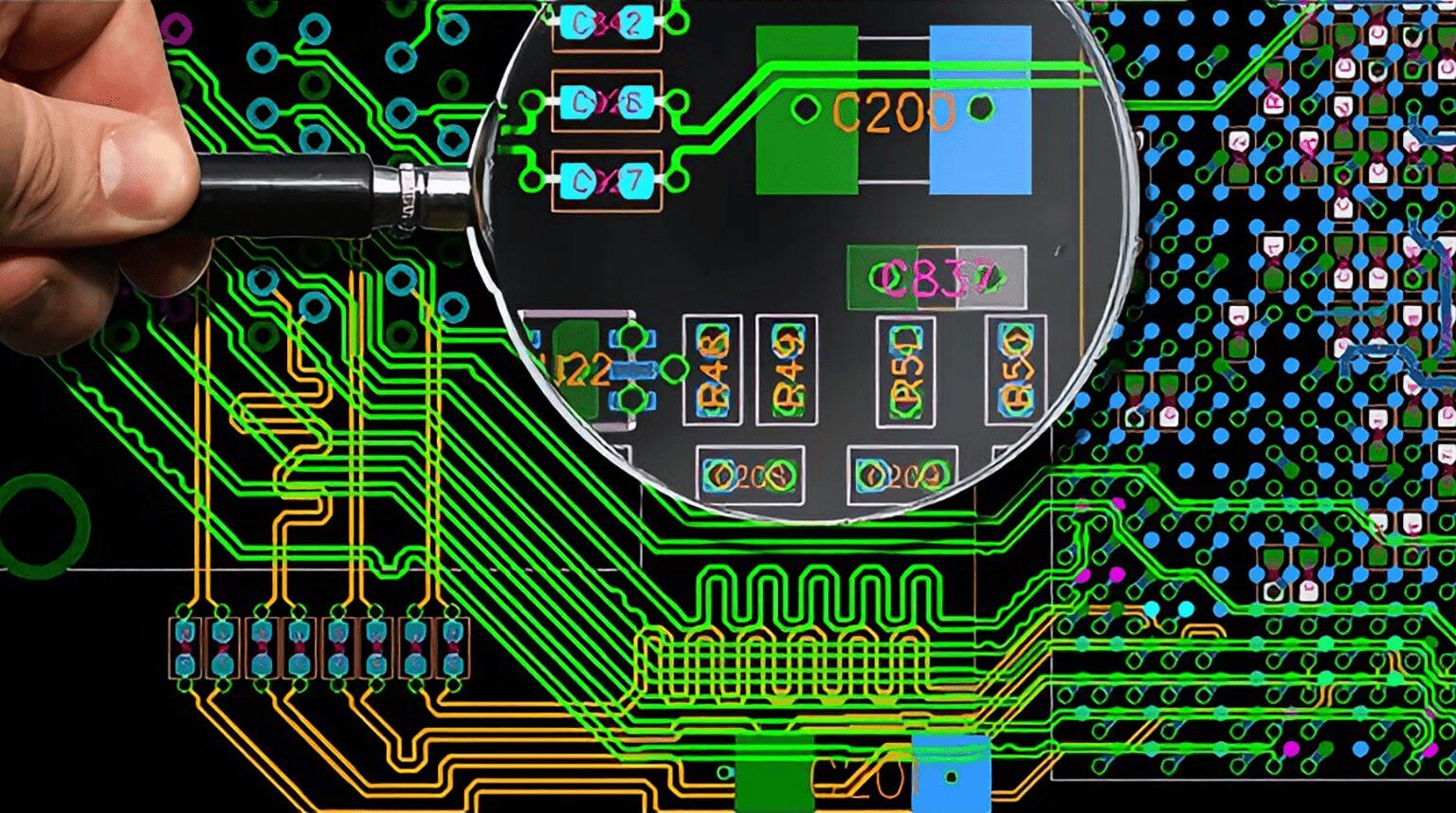
A 3/3 mil design means the trace width is 3 mil and the spacing is 3 mil. Since 1 mil equals 25.4 μm, 3 mil is about 76.2 μm. In other words, 3/3 mil is approximately 76 μm / 76 μm.
For many conventional PCB designs, this level of control is not required. Standard etching can be mature, efficient, and cost-effective. But when trace and space move down to 3/3 mil, the process window becomes much smaller.
At this level, a small difference in copper removal can affect the final trace width, spacing, or yield. If one area is etched too aggressively, the trace may become narrower than expected. If another area is etched too slowly, spacing may shrink or copper residues may remain.
Copper thickness also becomes more sensitive. Thicker copper usually requires longer etching time, which can increase the risk of side etching or undercutting. For fine-line PCB, the final result depends not only on the nominal trace/space value, but also on the relationship between copper thickness, etching parameters, and circuit density.
This is why PCBCool does not treat 3/3 mil HDI projects in the same way as ordinary PCB designs.
How Vacuum Etching Helps PCB Manufacturing
In a horizontal spray etching line, the top and bottom sides of a PCB panel may not behave exactly the same. On the top side, etchant can accumulate on the surface and create what is commonly known as the puddle effect. When spent etchant remains on the copper surface, it can slow down fresh etchant exchange and make copper removal less uniform.
For standard boards, this may not cause serious problems. For fine-line HDI boards, even small local differences can matter.
Vacuum-assisted etching helps by removing spent etchant from the board surface more effectively. This allows fresh etchant to reach exposed copper more evenly and supports a more stable reaction environment.
The practical benefits may include:
- More uniform copper removal
- Better line-width consistency
- Reduced risk of uneven etching
- Better support for fine trace and space
- Improved process control for PCB manufacturing
Vacuum etching does not eliminate all manufacturing risks. It does not completely remove undercutting, and it is not the only factor that determines whether a 3/3 mil PCB can be produced successfully. But for fine-line designs, it is a meaningful process capability because it helps control one of the most critical steps in copper pattern formation.
Typical Vacuum Etching Process Flow
The exact process may vary depending on factory equipment and board requirements, but a typical vacuum-assisted PCB etching flow can be understood as follows.
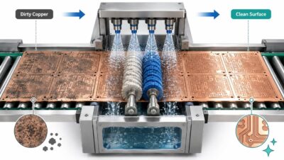
- Panel Preparation
Before etching, the PCB panel is cleaned and prepared for imaging. The copper surface must be clean enough to support stable photoresist adhesion and accurate pattern transfer.
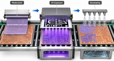
- Imaging and Developing
The circuit pattern is transferred onto the copper surface through photoresist, exposure, and developing. The copper that must remain is protected, while the copper to be removed is exposed.
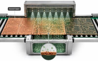
- Chemical Spray Etching
The panel enters the etching chamber, where chemical etchant is sprayed onto the exposed copper. The etchant reacts with the copper and removes it from the board surface.
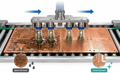
- Vacuum Extraction of Spent Etchant
The equipment uses a suction system to remove spent etchant from the board surface more actively. Instead of allowing used solution to remain on the copper surface and slow down the reaction, the vacuum system helps pull it away during horizontal processing.
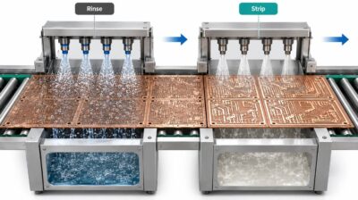
- Rinsing and Resist Stripping
After etching, the panel is rinsed to remove chemical residues. The remaining resist is then stripped away, leaving the designed copper circuit pattern.
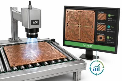
- Inspection and Process Feedback
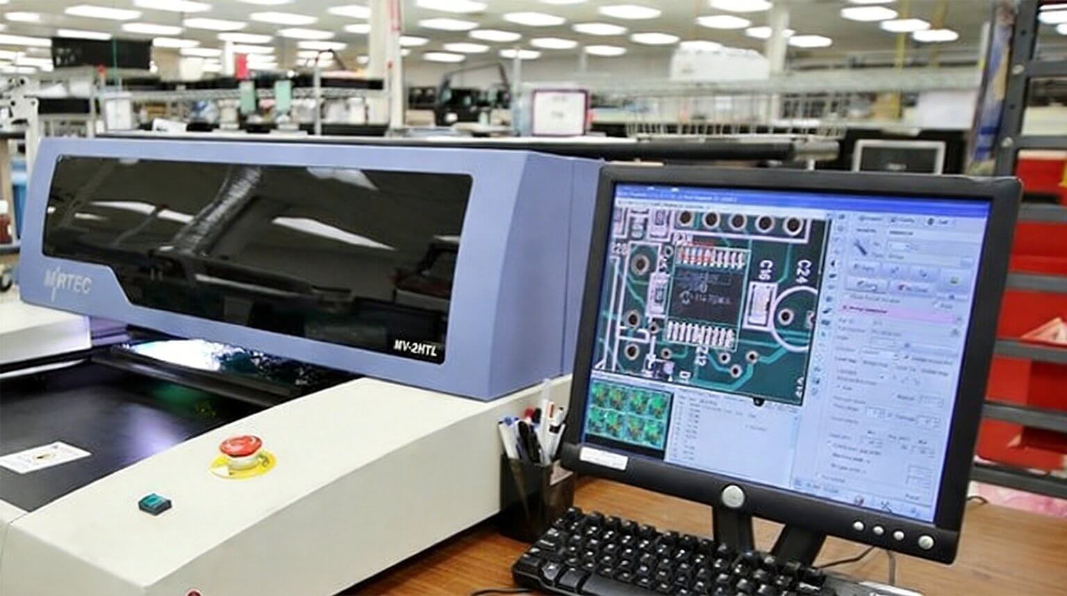
PCB require careful inspection after etching. The manufacturer may check final trace width, spacing, over-etching, under-etching, shorts, opens, and panel uniformity.
Vacuum Etching Is Only One Part of Manufacturing
Vacuum etching is important, but it should not be viewed as the only reason a manufacturer can produce fine-line PCB.
A stable PCB process also depends on:
- Substrate material selection
- Copper foil quality
- Copper thickness control
- Imaging resolution
- Developing control
- Etching compensation
- Lamination accuracy
- Registration control
- Cleanroom and contamination control
- AOI and final inspection
In other words, vacuum etching improves the etching stage, but final board quality still depends on the complete manufacturing control system.
This is also why engineers should not only ask, “Can you do 3/3 mil?” A better question is:
“What process controls do you use to manufacture fine-pitch HDI PCB consistently?”
Vacuum etching can be one part of that answer.
Final Thoughts
Vacuum etching is more than a machine feature. It reflects how a HDI PCB manufacturer approaches process control.
For simple boards, price and lead time may be the main concerns. For fine-line HDI boards, the question is different. Engineers need to know whether the manufacturer can control small geometry features repeatedly, not just produce one successful sample.
At PCBCool, vacuum etching is only one part of the solution. Before a demanding HDI project moves into production, our engineering team reviews the Gerber files, stack-up, copper thickness, trace/space requirements, impedance needs, and key manufacturing risks.
If a design is close to the process limit, we help customers evaluate the trade-offs and look for a more reliable manufacturing approach.
FAQs
A: No. It is mainly used when the design has fine trace/space, high routing density, or tighter line-width control requirements.
A: No. Vacuum etching helps improve etching uniformity and trace-width control, but the final result also depends on imaging, copper thickness, lamination, inspection, and other process controls.
A: Vacuum etching itself is not the main cost driver. The higher cost usually comes from the increased manufacturing difficulty, tighter tolerance control, and higher inspection requirements.
A: Thicker copper usually requires longer etching time, which can increase the risk of side etching or undercutting.
A: Yes, but indirectly. It helps maintain more consistent trace widths, while impedance is also affected by stack-up, dielectric thickness, material properties, copper thickness, and other factors.
A: No. Vacuum etching is still a subtractive copper etching process, but it improves etchant removal and exchange during wet etching.
A: No. It is mainly used to improve process control, not to shorten production time. For complex HDI boards, a reasonable lead time is often more important than an extremely fast turnaround.
A: Engineers should ask how the manufacturer controls fine-line production, including etching capability, copper thickness control, DFM review, impedance verification, and inspection methods.
Loki has worked in international trade and PCB since 2021, with experience in PCB fabrication, assembly, and customer communication. At PCBCool, he supports technical content publishing and helps connect customer inquiries with the right account manager for efficient project follow-up.