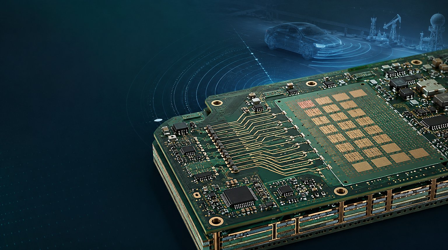
As PCB designs move from simple control boards to compact systems with dense components and high-speed interfaces, the stackup begins to affect much more than layer count. It can determine whether the board is easy to route, whether signals have stable return paths, and whether the design can be manufactured reliably.
When a standard multilayer structure no longer provides enough room to balance routing density and electrical performance, designers may begin to consider a higher layer count. However, adding more layers does not automatically create a better board.
This guide explains how engineers can plan an 8-layer PCB stackup for signal integrity, PDN performance, impedance control, and manufacturability.
A 4-layer or 6-layer PCB is often enough for many general electronic products. These structures work well when circuit density is moderate, the power structure is simple, and the design does not include demanding high-speed interfaces.
An 8-layer PCB becomes worth considering when a 6-layer layout can still be routed, but only with clear compromises. This may happen with dense BGA packages, FPGA-based circuits, multiple voltage rails, or stricter EMI requirements.
The value of an 8-layer stackup is not only the extra layer count. It gives engineers more room to separate signal groups and organize power and ground structures before moving to a more expensive 10-layer or 12-layer PCB.
Main advantages include:
- More routing space for dense layouts and BGA fanout
- Better reference-plane support for controlled impedance routing
- Improved return path control for high-speed signals
- More flexible power and ground plane planning
- Better separation between digital, analog, clock, and power circuits
- Better EMI and crosstalk control than lower-layer-count designs
In this sense, an 8-layer PCB is often the practical middle point between a limited 6-layer design and a higher-cost multilayer structure.
| Layer | Function |
|---|
| L1 | Signal |
| L2 | Ground |
| L3 | Signal |
| L4 | Power |
| L5 | Power |
| L6 | Signal |
| L7 | Ground |
| L8 | Signal |
This structure uses four signal layers, two power layers, and two ground layers. The signal layers are close to internal reference planes, which helps maintain shorter return paths and more predictable impedance behavior.
Configuration A is suitable for mixed-signal designs such as ADC/DAC boards, compact MCU systems, and PCB that combine digital and analog circuitry. It gives designers enough routing space to separate signal groups while keeping critical traces close to stable reference planes.
The main design consideration is power-plane partitioning. If the board includes several voltage domains, the power layers may need to be split, which increases the importance of decoupling, capacitor placement, and PDN review.
| Layer | Function |
|---|
| L1 | Signal |
| L2 | Ground |
| L3 | Signal |
| L4 | Power |
| L5 | Ground |
| L6 | Signal |
| L7 | Power |
| L8 | Signal |
This stackup places power and ground planes closer together to reduce loop area in the power distribution network. When dielectric spacing is properly controlled, this structure can support better transient current delivery and improved power integrity.
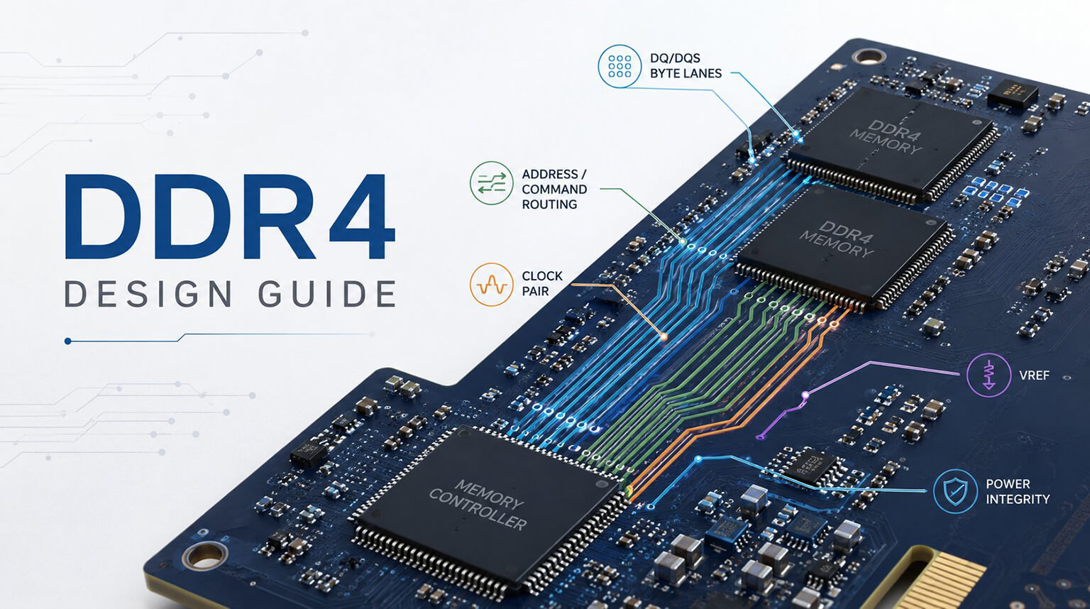
Configuration B is often used in high-speed digital or high-current designs, especially boards with FPGA, DDR4, PCIe Gen3, multi-core processors, or other devices that place higher demands on the PDN.
The trade-off is reduced routing and plane-planning flexibility. Plane splits, decoupling paths, and return current continuity need careful review.
| Layer | Function |
|---|
| L1 | Signal |
| L2 | Ground |
| L3 | Power |
| L4 | Signal |
| L5 | Signal |
| L6 | Power |
| L7 | Ground |
| L8 | Signal |
This structure focuses on mechanical balance. A more symmetrical stackup can help reduce warpage during lamination and reflow, especially in larger or thermally stressed PCB assemblies.
Configuration C is suitable for industrial controllers, dense assemblies, and boards with large or heat-generating components. It is useful when mechanical stability is as important as routing density.
The limitation is that some signal layers may not have ideal reference-plane adjacency. Designers may need to adjust dielectric thickness, trace geometry, or routing strategy to meet controlled-impedance requirements.
After the stackup is selected, designers need to decide how different signal groups are assigned across the available layers. The following example is based on an 8-layer PCB with high-speed digital interfaces such as DDR4 and PCIe Gen3.
Layer 1 is often used for critical high-speed signals such as PCIe differential pairs. Routing PCIe_TX_P/N and PCIe_RX_P/N on the top layer can reduce unnecessary via transitions and help preserve signal integrity.
If vias are required, symmetrical via placement and stub control become important for maintaining differential balance.
DDR4 address and command signals should use short, length-matched traces and stable adjacent reference planes. These signals may include DDR4_A0–A16, RAS#, CAS#, and WE#.
A practical approach is to place address and command groups on available inner signal layers where they can maintain consistent reference support and avoid unnecessary coupling with DDR4 data lines.
DDR4 DQ and DQS signals are high-speed digital signals that require strict routing control. They should be separated from switching control lines where possible and routed with stable impedance and length matching.
DQS pairs are especially important because they act as timing references for DDR4 data transfer. Consistent spacing, limited discontinuities, and predictable return paths help protect timing margin.
Layer 8 is often used for slower signals such as GPIO, low-speed control lines, configuration signals, and secondary routing.
These signals are less sensitive than DDR4 or PCIe traces, but they still need proper reference-plane planning. Slow signals can still create problems if they cross plane splits or pass through noisy power areas.
Continuous ground planes provide low-impedance return paths and help isolate high-speed and low-speed domains. When signal layers are close to ground planes, return currents can follow shorter and more predictable paths.
Many 8-layer PCB also include multiple voltage domains, such as 1.2V core power, 3.3V I/O, and 5V auxiliary power. Via placement, decoupling capacitor location, and plane boundaries should be planned to reduce noise coupling between voltage rails. In some designs, via spacing rules such as 10–15 mils may be used to reduce local impedance discontinuity and control coupling between domains.
Using dual power planes instead of a single power plane can improve PDN current delivery. When adjacent power and ground planes are separated by a dielectric thickness of less than 4 mils, PDN loop inductance can be reduced by about 40% under controlled stackup conditions.
This close power-ground coupling can help deliver fast transient current to FPGA, DDR4, and processor power rails. In some design conditions, plane-to-plane impedance can be kept below 5 milliohms at frequencies above 100 MHz.
Many 8-layer PCB need to support multiple voltage domains, such as 1.2V core power, 3.3V I/O, and 5V auxiliary power. These domains may share the same ground reference, but their power regions and via allocations still need to be carefully controlled.
Keeping via spacing in the range of 10–15 mils between different power domains can help reduce local impedance discontinuity and limit noise coupling between voltage rails. Plane splits, via placement, and decoupling paths should be planned together to keep each supply path stable and well referenced to ground.
Thermal via arrays can help transfer heat from regulators, MOSFETs, and high-current components into internal copper planes.
For example, arrays of 10 mil thermal vias spaced 12–15 mils apart can improve heat dissipation from regulators and MOSFETs. In some design conditions, 100 thermal vias may provide about 0.08–0.12°C/W of thermal resistance reduction.
The actual thermal benefit depends on board thickness, copper weight, via plating, copper plane connection, and heat source size.
For DDR4 interfaces, PDN and return path design directly affect timing margin and simultaneous switching noise. In the design basis described here, keeping return path inductance below 0.5 nH/inch helps reduce simultaneous switching noise during DDR4 operation.
This requires continuous reference planes, short via paths, proper decoupling placement, and careful separation between power domains.
Routing the DDR4 data bus on an 8-layer PCB requires careful impedance and length control to maintain setup and hold margins at multi-gigabit rates.
As a general design basis, single-ended DDR4 DQ traces may use a width range of 5 to 8 mils, with about 3.9 mil dielectric separation to the adjacent reference plane, to maintain a target impedance of 50Ω. The final trace width should still be confirmed based on the actual stackup, dielectric constant, copper thickness, and solder mask condition.
For length matching, unbuffered DIMM interfaces may allow a tolerance of about ±5 mil, while registered DIMM interfaces at higher clock frequencies may require tighter control, such as ±2 mil. These tolerances help control propagation delay skew between byte lanes and reduce the risk of timing failure during simultaneous read/write transitions.
Address and control signals should be separated from noisy or fast-switching signal groups. In one routing approach, command signals such as A0–A15 may be routed on one inner signal layer with 6 mil traces, while RAS#, CAS#, and WE# may be isolated on another layer with 5 mil traces.
At 1 GHz, a 5 mil trace with 3.9 mil dielectric separation can produce a coupling coefficient worse than 0.35 when spacing is insufficient. Separating command buses by layer can reduce near-end coupling and help minimize timing ambiguity or false rank-selection events.
PCIe Gen3 differential routes typically use around 8 mil trace width and 3 to 4 mil intra-pair spacing to maintain 100Ω differential impedance, depending on the actual stackup.
Pair skew should be controlled within about ±10 mil. When vias are required, back-drilling or controlled-depth drilling may be needed to reduce residual via stubs to about 5 mil, since stub resonance can become a major discontinuity above 4 GHz.
PCIe Gen4 requires tighter routing control than PCIe Gen3. In the original design basis, PCIe Gen4 routing requires differential coupling length greater than 800 mil while maintaining receiver eye openings of 180 mV or higher.
These values should be confirmed through simulation and the relevant chipset or interface design guide.
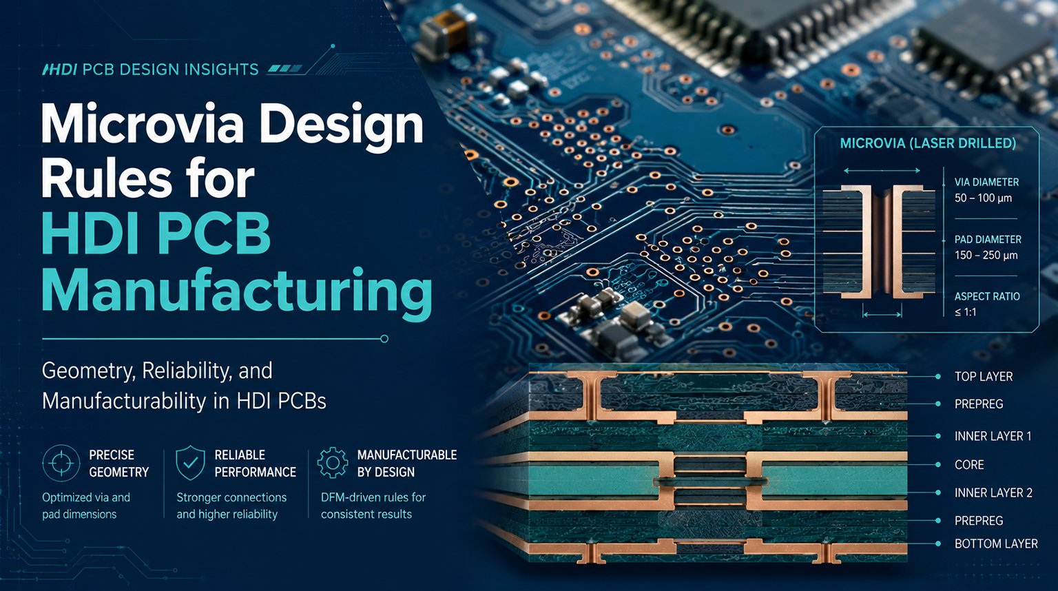
Blind vias can reduce stub-related reflections compared with through vias, especially in high-speed 8-layer designs where discontinuities above 100 MHz become more important.
For signal vias, the average parasitic capacitance may be estimated at about 0.8 pF. Symmetrical via placement between differential pairs is important for maintaining pair balance and impedance continuity.
Through-via aspect ratio is one of the main manufacturing constraints in 8-layer PCB. A common range is 8:1 to 12:1, depending on board thickness, drill diameter, plating capability, and reliability requirements.
If the aspect ratio is too high, drilling accuracy, plating uniformity, and long-term reliability may be affected. Higher aspect ratios can also increase cost because they require tighter process control.
Prepreg thicknesses between 0.003 and 0.007 inch and core thicknesses between 0.031 and 0.062 inch may influence achievable via depth, drill size, and impedance range.
Blind vias can reduce stub reflections and support high-density routing, but they are more expensive than standard through vias.
In DDR4 and PCIe Gen3 designs, blind vias may increase PCB cost by 40% to 50% compared with through-via structures, depending on lamination steps, laser drilling requirements, yield, and supplier capability.
Blind vias should be selected for clear design needs, such as high-density BGA breakout, signal-integrity improvement, or routing limitations.
Copper weight affects both current capacity and manufacturability. Half-ounce copper can support finer traces, such as 3 mil traces for high-density BGA fanout, but it has lower current-carrying capacity.
Two-ounce copper can support higher current, but it usually requires wider traces and larger spacing. In some processes, 2 oz copper may require minimum trace widths around 8 mils while allowing trace currents above 15 amps.
Thicker copper also makes etching control more difficult, which can affect impedance accuracy.
A symmetrical stackup helps reduce warpage after reflow. This is especially important for large boards, thermally stressed designs, or assemblies with dense components such as FPGA and DDR4 devices.
Copper distribution should be balanced across the stackup where possible. Uneven copper loading can create stress during lamination and assembly.
Design Rule Checks, or DRC, define manufacturable limits for trace width, trace clearance, via diameter, annular ring, solder mask clearance, and copper spacing.
DRC rules should be based on the PCB manufacturer’s actual process capability. Copper thickness tolerance and dielectric constant variation can affect impedance and final electrical performance.
Setting realistic DRC limits early helps reduce manufacturing defects and avoids costly prototype rework.
A reliable PCB is not defined by layer count alone. It depends on stackup planning, impedance control, return paths, PDN design, via structure, and manufacturability working together from the beginning.
PCBCool supports PCB manufacturing from 1 to 40 layers, including controlled-impedance boards, HDI PCB, high-speed digital boards, and complex multilayer designs. Whether your project involves DDR4, PCIe, FPGA, dense BGA fanout, or difficult fabrication requirements, our engineering and manufacturing teams can help make it buildable.