Perhaps you already know that the circuits on a Printed Circuit Board (PCB) are designed using layout software. However, if you’re not familiar with PCB manufacturing, you might assume that the design files are directly used to build the boards. In reality, manufacturers don’t use those design files directly. Instead, they rely on a specific set of manufacturing files called Gerber files.
If you’re not familiar with Gerber files, this article is perfect for you. PCBCool will explain PCB Gerber files in an easy-to-understand and practical way, focusing on their role in real-world manufacturing, and offering tips to help designers avoid common mistakes.
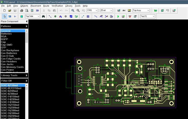
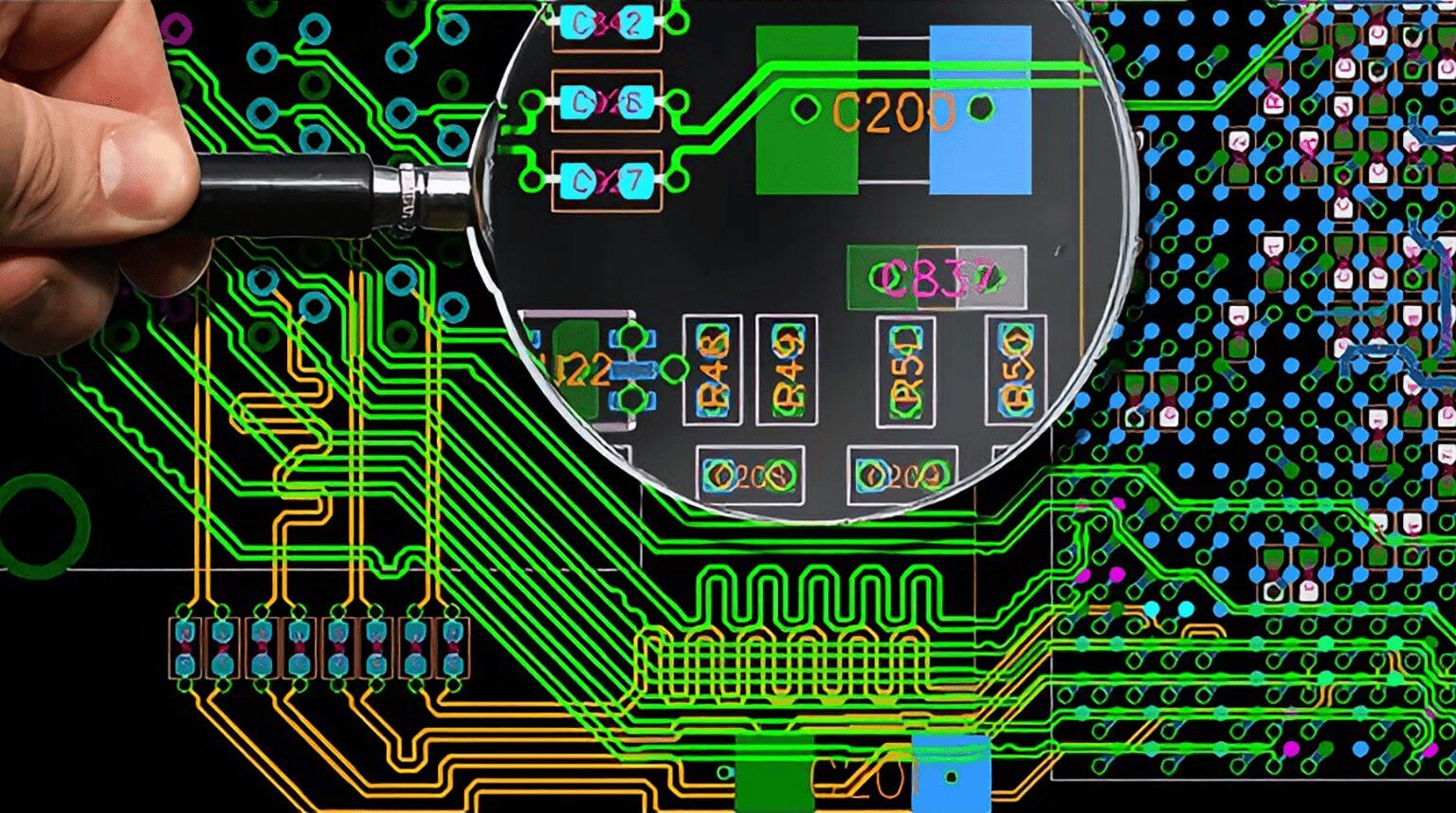
Gerber files are 2D manufacturing files that describe every physical layer of a PCB. They sit at the boundary between design and manufacturing, acting as the bridge that translates design intent into instructions that fabrication machines can follow. Each Gerber file represents one specific layer of information, such as copper traces, solder mask openings, silkscreen markings, or the board outline.
Unlike PCB design files, Gerber files don’t contain design rules or intelligence. Instead, they provide detailed instructions on what should be printed, etched, or cut on each layer of the board.
Once the Gerber files are generated, the PCB manufacturer uses them as the single source of truth for fabrication. If something is missing or incorrect in the Gerber files, it can result in errors in the final product—even if the original design was perfect.
Errors in Gerber files can lead to a range of issues, such as missing connections, short circuits, incorrect board shapes, unusable silkscreen, or even production delays. This highlights the critical importance of ensuring Gerber files are error-free. Just like schematic and PCB layout files, Gerber files deserve the same level of careful attention during the design and verification process.
A standard PCB project typically includes multiple Gerber files, each serving a specific purpose.
Copper Gerber files define the electrical connections on the board. These include the top copper layer, bottom copper layer, and any inner layers for multilayer boards. They show traces, pads, vias, and copper pours.
Solder mask Gerbers define where solder mask is applied and where copper is exposed. Openings in the solder mask allow soldering, while covered areas protect copper and help prevent solder bridges.
Silkscreen layers contain printed markings such as component reference designators, polarity indicators, logos, and assembly notes. These markings assist with assembly, inspection, and debugging.
The board outline layer defines the exact shape and size of the PCB. This information is used by the manufacturer to route the board out of the panel. An incorrect or missing outline can cause serious fabrication issues.
Drill files specify the locations and sizes of all holes on the PCB. They also indicate which holes are plated and which are not. Drill files are typically provided in Excellon format and are always included alongside Gerber files.
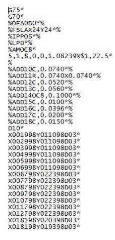
Modern PCB designs use the RS-274X Gerber format, which has become the industry standard for PCB fabrication. Unlike older formats, RS-274X embeds all the required information directly into each file, including aperture definitions, which are critical for accurately describing features like pads and traces. The following is an example of RS-274X:
In older Gerber formats, aperture definitions were stored in separate files, often leading to errors and confusion during the manufacturing process. This separation meant that if an aperture file was missing or incorrectly linked, it could result in discrepancies between the design and the final product. RS-274X solved this issue by making the aperture definitions part of the Gerber file itself, ensuring that all necessary information is contained in one place.
One of the key advantages of RS-274X is that it is self-contained, meaning that it includes all the data required for fabrication, without needing external references. This makes the file easier to manage, share, and verify. Because of this, RS-274X is reliable and widely supported by PCB manufacturers, making it the go-to format for most modern PCB designs.
Additionally, RS-274X supports more complex designs, such as those with finer features or multi-layer boards, and it offers greater precision in defining features like pads, vias, and traces. This level of detail is crucial in modern electronics, where high-density, high-performance PCBs are required.
Gerber files are exported from PCB layout software once the design is complete. This export step is critical and should never be rushed.
Designers must verify the following:
- Correct layer selection
- Proper units
- Correct polarity for solder mask layers
- Inclusion of all required files
Relying solely on default export settings can lead to mistakes, so double-checking these details is essential for a smooth fabrication process.
When a PCB manufacturer receives Gerber files, the first step is to load them into CAM (Computer-Aided Manufacturing) software.
The CAM process involves several critical stages, including:
- Data Verification
- Imaging
- Drilling
- Plating
- Routing
- Quality Checks
- Assembly Preparation
If all the data in the Gerber files is accurate and complete, the manufacturer can proceed without issues. However, if something is unclear or missing, the manufacturer will typically reach out to the designer for clarification, ensuring that the final product is as intended.
Some common mistakes found in Gerber files include:
- Missing board outlines
- Incorrect layer polarity
- Silkscreen printed on pads
- Misaligned drill data
- Mirrored bottom layers
- Copper features placed too close to the board edges
Many of these issues aren’t visible in the PCB design software and only become apparent during manufacturing.
Good practices for creating clean Gerber files include:
- Using clear and consistent file naming conventions
- Always including drill files
- Exporting Gerber files fresh for every revision
- Visually reviewing all files before release
Gerber files should clearly communicate the design intent without requiring interpretation or guesswork.
Gerber files are the final and most important output of a PCB design. They define exactly how a board will be manufactured, layer by layer.
By understanding what Gerber files represent, how they are used in fabrication, and how to properly verify them, designers can avoid costly errors and ensure their PCBs are manufactured correctly on the first attempt.
A well-prepared Gerber package reflects a professional and production-ready PCB design.
At PCBCool, we specialize in providing high-quality PCB manufacturing, assembly, and Gerber file verification services. If you’re looking for reliable, precision-driven PCB solutions, we’re here to help you turn your design into a flawless product, every time.