
Blog

What Is Laser Drilling in PCB Manufacturing

0
Laser Drilling in PCB Manufacturing

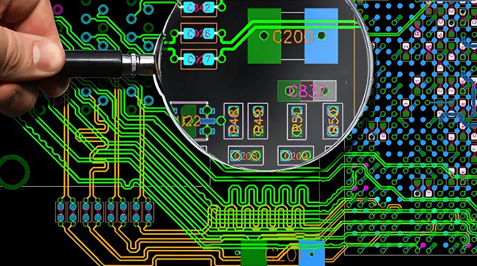
When we open an electronic device, one of the first things we usually notice is a PCBA densely populated with components. These components are not simply attached to the circuit board. They depend on different holes and vias for mounting, support, and electrical connections between layers.

As PCB designs become smaller and more densely routed, the requirements for these holes have also changed. In many advanced boards, especially HDI, the challenge is no longer only to drill a hole. The manufacturer must create small, accurate, and plateable vias within a very limited space.

This is where laser drilling becomes important. It is widely used to form microvias for high-density routing, via-in-pad designs, and staggered via structures.

What Is Laser Drilling in PCB Manufacturing

PCB drilling aims to create various types of holes or vias. In conventional PCB manufacturing, many of these holes are formed by mechanical drilling, where a rotating drill bit cuts through copper, resin, glass fiber, and other laminate materials.

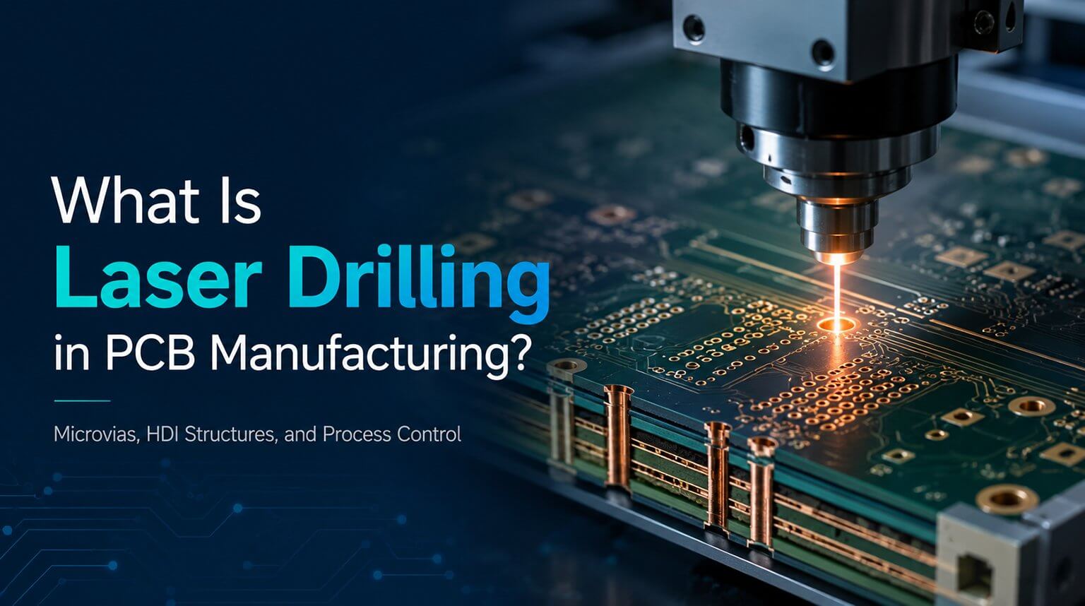
Laser drilling uses a different method. Instead of cutting the material with a physical drill bit, it uses focused laser energy to remove material through ablation. During ablation, the material absorbs laser energy and is rapidly heated, decomposed, vaporized, melted, or ejected from the drilling area.

In manufacturing, CO₂ lasers and UV lasers are commonly used under different process conditions. CO₂ lasers are often used for dielectric removal, while UV lasers can provide finer energy control and may be used for smaller features or more delicate material interaction.

Why Laser Drilling Is Crucial for Advanced PCB

Mechanical drilling remains reliable and efficient for many standard PCB applications, including through holes, larger vias, and mechanical mounting holes.

However, the hole size is directly tied to the drill bit size. A smaller hole requires a thinner drill bit. As the bit becomes thinner, it becomes more fragile and more sensitive to wear, vibration, deflection, and breakage. These issues can affect hole accuracy, wall quality, registration stability, and production efficiency.

Laser drilling avoids this specific limitation because it does not rely on a physical cutting tool. There is no tiny drill bit pressing into the laminate, so the process is not restricted by drill bit strength or tool breakage in the same way. This makes laser drilling better suited for very small blind and buried vias where mechanical drilling becomes difficult to control consistently.

For advanced PCB, this capability is important because microvias help reduce routing space and support compact layer transitions. They are commonly used in HDI stack-ups such as 1+N+1, 2+N+2, stacked or staggered vias, and via-in-pad designs.

Mechanical Drilling vs. Laser Drilling

Item Mechanical Drilling Laser Drilling
Processing Method Physical cutting with a rotating drill bit Non-contact ablation using focused laser energy
Typical Use Through holes, larger vias, mechanical holes microvias, blind vias, via-in-pad structures
Hole Size Capability Limited by drill bit strength, tool life, and process stability Suitable for smaller vias and dense HDI layouts
Tool Wear Drill bits wear and may break No mechanical drill bit wear at the hole
Main Process Risk Burrs, drill wander, bit breakage, smear Under-drilling, pad damage, residue, carbonization
Material Interaction Cuts copper, resin, and glass mechanically Different materials absorb laser energy differently
Process Control Focus Drill bit quality, spindle accuracy, feed rate, registration Laser energy, focus, pulse control, alignment, cleaning, plating

Key Manufacturing Controls in Laser Drilling

Laser drilling quality is not determined by a single equipment setting. It is closely tied to both microvia design and process control. The following are some of the key factors that need to be considered:

Control Factor Why It Matters
Via Diameter Smaller vias save routing space but require tighter alignment, cleaning, and plating control.
Dielectric Thickness Thicker dielectric increases via depth and can make plating more difficult.
Aspect Ratio A deep, narrow via is harder to plate reliably than a shallow one.
Copper Thickness Copper thickness affects copper window formation, laser response, and target pad integrity.
Capture Pad and Target Pad Design Insufficient pad size reduces registration margin and increases connection risk.
Laser Type CO₂, UV, or combined laser processes may be selected depending on the dielectric and copper structure.
Laser Energy Control Power, pulse duration, frequency, focus, and pulse count affect hole profile and thermal impact.
Optical Alignment Camera or CCD alignment helps the via land accurately on the target pad.
Post-Drilling Cleaning Plasma cleaning, desmear, and micro-etching help remove residue before metallization.
Copper Plating The drilled via must be plated without voids, thin copper, or weak bottom connection.
Inspection AOI, X-ray, microsection, and electrical testing help verify via quality and continuity.

For this reason, an HDI PCB supplier should not be evaluated only by its minimum laser drilling diameter. The more important question is:

Whether the factory can control the entire microvia process from drilling to plating and inspection.

Different Laser Drilling Methods

4 Different Laser Drilling Methods

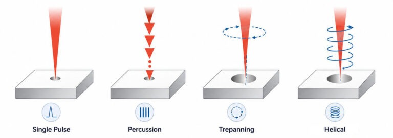
Different laser drilling methods may be used depending on the required via diameter, depth, material, and hole profile.

  • Single-Pulse

Single-pulse drilling uses one laser pulse to form the hole. It is fast, but it offers limited depth control and is not always suitable for more demanding via structures.

  • Percussion

Percussion drilling uses multiple laser pulses at the same location. Each pulse removes additional material until the required depth is reached.

  • Trepanning

Trepanning moves the laser beam around a defined circular path. It is useful when the required hole diameter is larger than the beam diameter.

  • Helical

Helical drilling moves the laser beam in a spiral or helical path. It can improve control over hole geometry in certain applications, although it is more complex.

How the Laser Drilling Process Works

  1. Data Review

Before production, PCBCool’s engineering team reviews the stack-up, drill file, and via structure. This review determines whether the design is manufacturable and whether the microvias can be plated reliably.

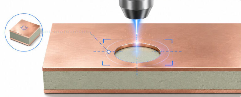
  1. Copper Window Formation

In some laser drilling processes, especially when a CO₂ laser is used to remove dielectric material, the copper surface may need to be opened before ablation. This opening is often called a copper window.

Copper Window Formation
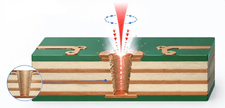
  1. Laser Ablation

During laser ablation, the laser removes dielectric material and forms the microvia cavity.

The main process parameters include beam focus, laser power, pulse duration, pulse frequency, pulse count, energy distribution, positioning accuracy, and drilling depth.

Laser Ablation
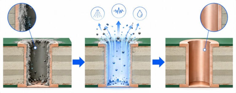
  1. Debris Removal and Desmear

Laser drilling can leave residue inside the via such as resin residue, carbonized material, glass fiber particles, or debris on the exposed target pad.

Depending on the material and process, preparation may include plasma cleaning, desmear, chemical cleaning, micro-etching, or surface activation.

Debris Removal and Desmear
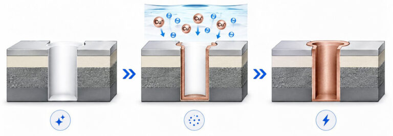
  1. Electroless Copper and Copper Plating

After drilling and cleaning, the via must be made conductive. This is typically done through electroless copper deposition followed by copper plating.

Electroless Copper and Copper Plating
  1. Inspection and Reliability Verification

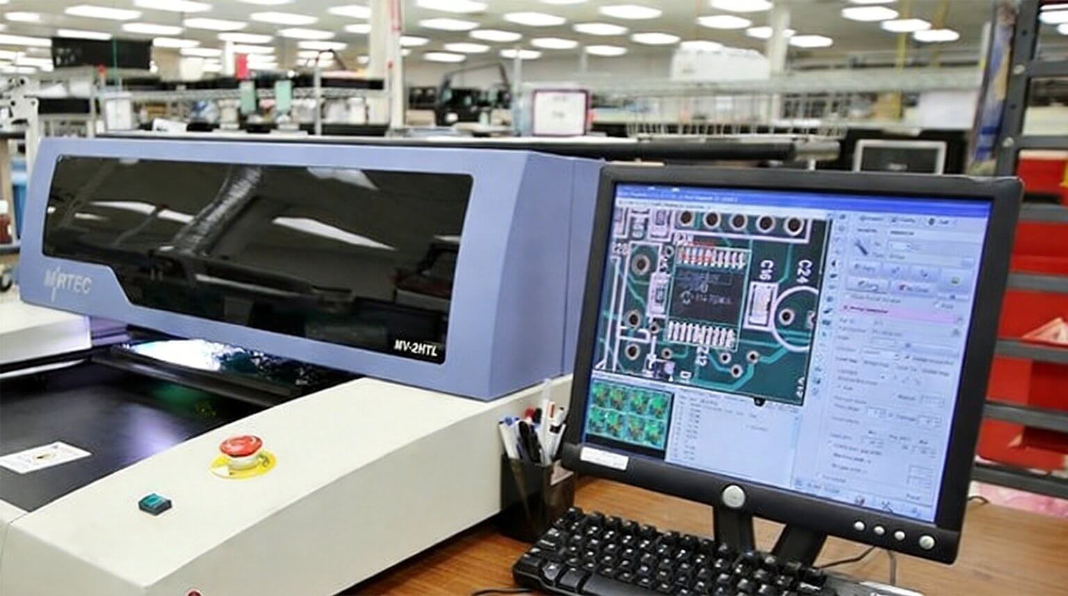
Inspection may check via diameter, position, depth, shape, target pad contact, plating continuity, plating thickness, via wall cleanliness, voids, pad damage, and electrical continuity.

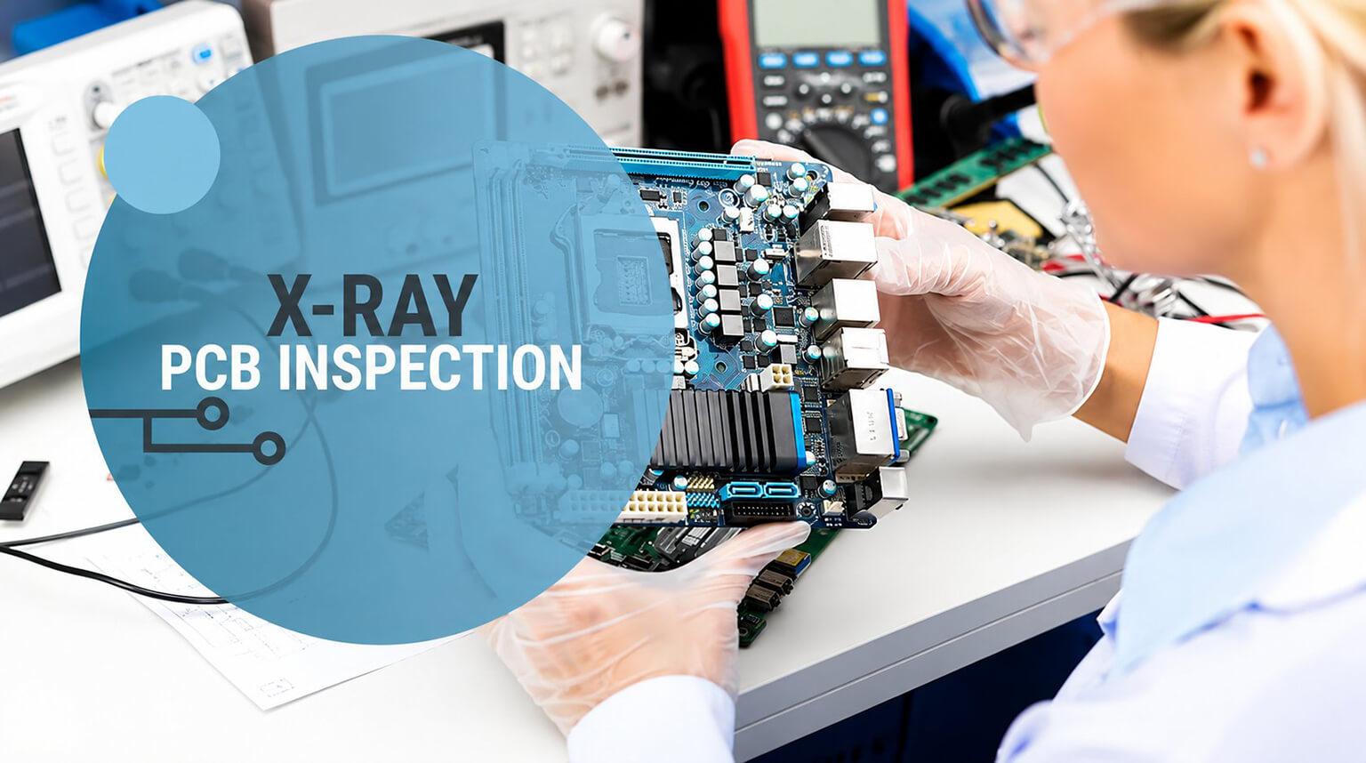
Common inspection methods include AOI, X-ray inspection, microsection analysis, electrical testing, and reliability testing, depending on the project requirements.

For critical HDI boards, microsection analysis is especially useful because it shows the actual via profile, plating condition, and connection to the target copper pad. It can reveal defects that are not visible from surface inspection alone.

Final Thoughts

For engineers and electronics manufacturers, the value of laser drilling is not only smaller hole size. It allows PCB designs to move into higher-density structures while still maintaining manufacturability at the production level. In this sense, laser drilling represents more than a drilling method; it is part of the manufacturing foundation behind advanced PCB design.

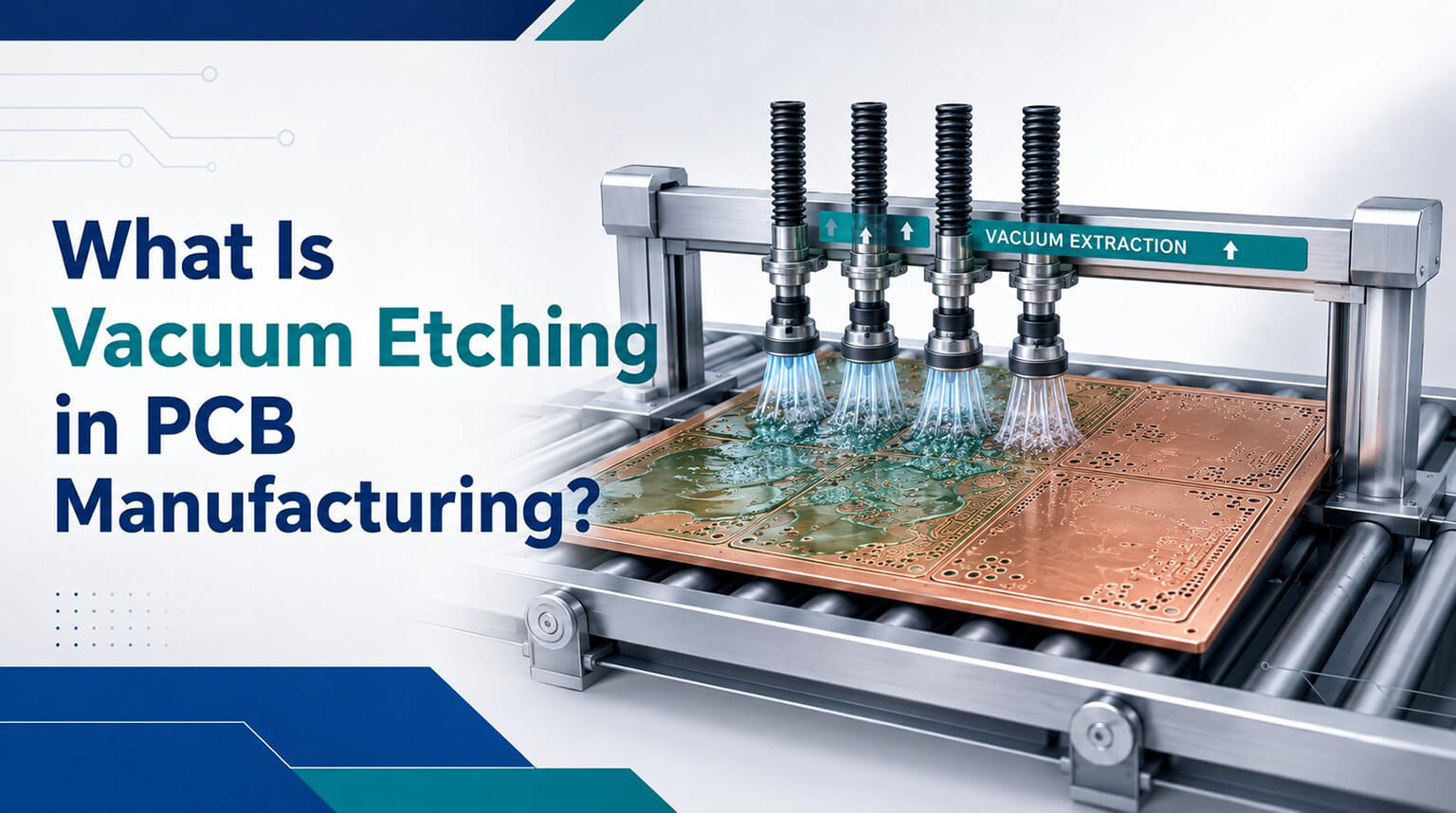
If your project involves HDI PCB, laser-drilled microvias, via-in-pad structures, or fine-line circuit requirements, PCBCool can support the manufacturing process. Our facilities are equipped with vacuum etching and laser drilling machines, helping us handle complex PCB projects that require both via precision and fine-line circuit control.

FAQs

Q1: Is Vacuum Etching Required for Every HDI PCB?

A: No. It is mainly used when the design has fine trace/space, high routing density, or tighter line-width control requirements.

Q5: Can Vacuum Etching Help with Impedance Control?

A: Yes, but indirectly. It helps maintain more consistent trace widths, while impedance is also affected by stack-up, dielectric thickness, material properties, copper thickness, and other factors.

Loki
Loki | International Trade and PCB Manufacturing Specialist

Loki has worked in international trade and PCB since 2021, with experience in PCB fabrication, assembly, and customer communication. At PCBCool, he supports technical content publishing and helps connect customer inquiries with the right account manager for efficient project follow-up.

Related Tags