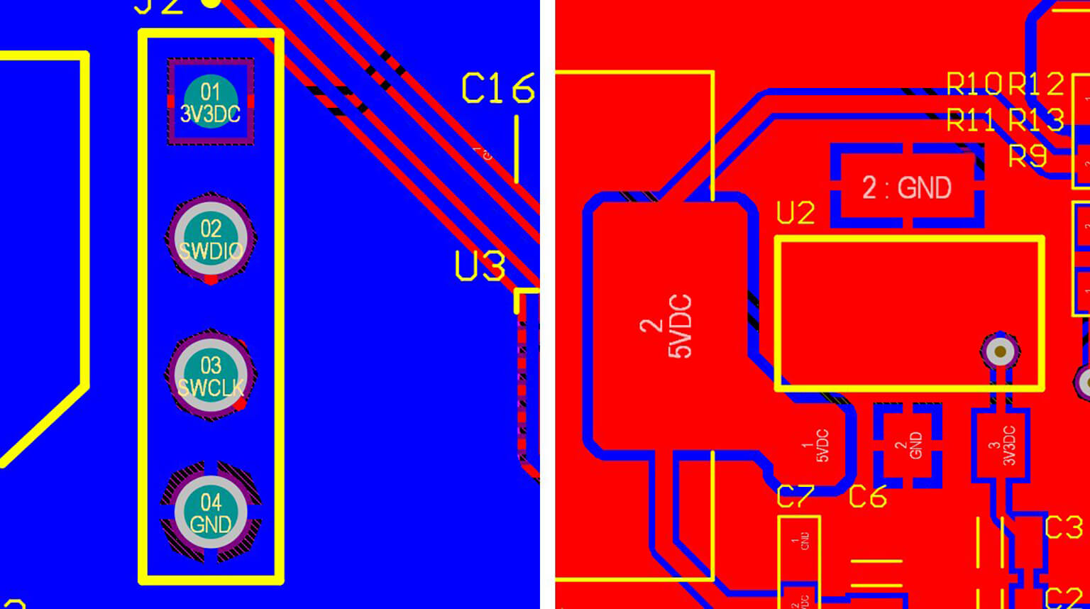
When examining PCB layouts, many people consider stitching vias to be insignificant because they are usually represented as small repetitive objects arranged in a repetitive manner, often resembling an industrial pattern.
Most engineers will use stitching vias once they have completed routing their PCB and have filled in copper. They will typically add a few stitching vias along the periphery of the PCB and will consider it acceptable. They do not always work; therefore, it is important to use stitching vias properly.
Most do not recognize that stitching vias are part of the PCB’s electromagnetic structure and will control the return paths. They will reduce electromagnetic interference (EMI) emissions from the circuit board (PCB), increase thermal conductivity of the copper, and even provide additional mechanical stability to the PCB. Once engineers view stitching via as a structural element to their PCB, they will begin to see improved performance on their PCBs.
This article does not provide rules for using stitching vias as they pertain to general design guidelines but rather provides reasoning behind why stitching vias are important and how to properly use them.
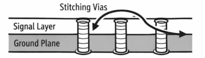
In basic terms, a stitching via is used to connect copper areas together between layers on a PCB. More specifically, it connects ground planes typically smashed during multi-layer PCB designs; however, this simple explanation does not convey much about the intent of the stitches.
Ground planes created by multi-layer PCB designs will have multiple layers of connections; if there were no stitching via, then there would only be a couple of points of connection between those planes (Die pads and mounting pads). This will cause the ground plane to behave incorrectly due to the fact that current flow may be uneven, as well as cause impedance problems.
Stitching vias aids in the establishment of low impedance paths vertically between layers on the board. This vertical connection serves some critical functions.
One is to improve the flow of return current, high and fast signals and digital logic levels rely heavily on a continuous reference plane for proper operation, if there’s no reference plane or a gap in the reference plane then the return signal will have to travel further, which may create a high EMI surrounding the trace due to increased loop area, thus creating misbehavior. A stitching via will reduce the overall length of the vertical current loop, thus lowering the respective inductive impedance.
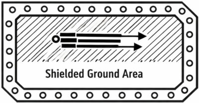
The second item is to keep the transmission of an electromagnetic field. A stitching via will act as a fence around a high-speed trace or a board’s edge and virtually eliminate radiation and reduce the board’s susceptibility.
Once the impact of stitching via’s detail is understood (current loop control and electromagnetic field containment), a design will no longer be developed with a random method of performing this function.
The assumption that the return current on a circuit board spreads evenly throughout the ground plane can lead to issues in the design of the board. In reality, the return current does not evenly spread out when it returns from the load to the source, the return current travels the path of lowest impedance, which will generally be vertically downwards through the ground plane under the signal trace, creating a vertical return current path.
When the signal trace goes from one side of the board to the other via a via hole, there is a potential for there to be no return current path, since on either side of the via hole is a different reference plane. In this case, the return current is forced to travel laterally across the reference plane to find the nearest connection to return to the source, and as a result, the loop area increases. The increase in loop area translates to increased radiation and noise being emitted from the load.
To minimize EMI, if you place stitching vias close to the signal via, then you will be providing a vertical return path for the return current. The addition of the stitching via will significantly decrease the EMI problems. Stitching via location is found after engineers have failed EMC testing; they then make the necessary modifications and see a drastic decrease in emissions.
Board edge stitching is widely seen in RF & high-speed digital designs.
Looking at RF boards, you can typically see a row of ground vias as the perimeter/edge of the PCB. As stitching vias are located along the edges, you create a quasi-cavity structure (the top and bottom ground planes are connected at regular intervals, thus forming a barrier to edge radiation).
This is of particular importance in faster edge designs, such as DDR, PCIe, USB 3.x, or RF transmitters. Even if your design is not strictly RF, fast digital signals will act like RF signals.
Spacing matters here because if the vias are spaced too far apart, they will no longer perform as a fence. A good rule of thumb for spacing is to keep spacing below 1/10 of the wavelength of the highest frequency of concern. However, many designers use spacing between 2mm and 5mm, depending on their design constraints.
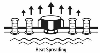
Most of the time, when we talk about stitching vias, we focus on EMI issues. However, stitching via help thermally as well. Copper planes can spread heat throughout the board; however, if you make heating on one copper layer and if the copper on another layer is not properly connected to the first layer, the heating will not spread out as efficiently.
By placing stitching via’s in high-power areas of the circuit, you will create a vertical thermal path or the ability for heat to flow vertically through the several copper planes, as well as just horizontally. Now, these vertical thermal paths can really help in power devices, such as MOSFETs, voltage regulators, and LEDs.
In certain instances, designers will place an array of thermal vias directly underneath pads. Technically, this will not provide the same types of stitching as ground stitching around the perimeter of the board. Still, it does provide a similar benefit of having multiple vias all connected to provide vertical conductivity.
So when considering hot spots on your PCBs, don’t just think about applying more copper, think about connecting all copper traces and layers vertically.
Signal integrity and EMI in high-speed routing are interrelated. When a trace on a reference plane is continuous (no splits), the fields from the trace remain mostly confined to the area above it. Once the reference plane is broken or the trace crosses a split, the fields will no longer be contained.
As an example, when routing differential pairs along a layer that changes from a continuous reference plane, if stitching vias are placed close to the differential trace to provide local return paths, signal integrity is improved. Some designers will put via fences beside the traces in RF applications in addition to the returned paths. This stitching technique will reduce the amount of crosstalk and improve isolation between sensitive circuits.
If stitching is done excessively, the overall cost and complexity of manufacturing will increase. It is all about balance, similar to all aspects of PCB design.
In layout software, it’s easy to create stitching vias; however, adding stitching vias adds to the time required to drill them and can have a negative impact on the yield of the product.
Very dense via fences will increase costs for manufacturing as well. If you add microvias, costs will increase even further. Additionally, placing too many vias near the edges of the board could potentially compromise the structural integrity of the board if they are not spaced correctly.
To avoid any issues, it is important to contact your PCB manufacturer early and ask about the minimum drill size, the aspect ratio limitations, and the annular ring requirements.
Stitching vias must be electrically functional and able to be manufactured. If you design a stitching that cannot be produced consistently and dependably, there is no value in designing it.
Not every board ought to be over-designed with aggressive stitching. Most lower-speed two-layer circuit boards will perform well without a dense set of stitching vias. For example, ground planes and copper pours on two-layer printed circuit boards are often sufficient to achieve good circuit performance.
Overdesigning a printed circuit board can inflate costs without improving performance; therefore, the engineering maturity required to know when to apply the technique is as important as the engineering maturity required to know when not to apply the technique.
The significance of sewing via stitch as a part of EMC testing is also understood by numerous engineers.
There are instances where a board tests successfully in a laboratory setting but only to subsequently fail radiated emissions testing. Examples of simple remedies are copper tape, additional ground wires, or redesigning with a sufficient amount of stitching.
Most likely, ground continuity issues are the primary reason for these failures. Boards that pass EMC regularly, have a great deal of attention to detail with respect to their ground stitching and typically include grounding at or near connectors and edges of boards, as well as an appropriate amount of grounding in the high-speed areas.
It is more economical to properly design the stitching during the initial phases of development, rather than redesign the product after it fails.
An additional advantage that usually isn’t taken into consideration is the mechanical support provided by stitched vias. Stitched vias can help to provide mechanical integrity by stitching multiple layers together, which reduces the possibility of large copper blocks in a PCB delaminating or flexing due to thermal cycling.
In automotive and industrial environments that are prone to vibration, this extra mechanical support helps increase the longevity and reliability of a PCB.
Again, this is not the primary purpose of stitched vias, but it is a bonus.
The first error is generally putting in stitching vias at random, after the routing is done. By not understanding where the current is flowing, stitching vias can sometimes not be of any assistance.
Secondly, some engineers insert stitching vias too far away from an adjacent signal transition. A stitching via that is 10 mm away from the signal via will be unable to effectively return current.
A third common error is forgetting to add stitching vias to power planes on occasion. The ground reference is not the only reference on the board.
Finally, some engineers will overuse stitching vias, making it difficult to route and increasing board cost significantly.
Last but not least, through-hole stitching vias are small components that play very large roles in a circuit by affecting EMI performance, affecting signal integrity, providing thermal dissipation, and contributing to mechanical strength. They are not a thing of beauty, nor are they visually enticing in pictures used for advertising purposes. However, they are often associated with an accomplished PCB designer.
Professional engineers do not include stitching vias based on a written requirement. They include them because they possess knowledge of the direction of the current and the conductance pattern from the field. Stitching vias reflects deeper characteristics about PCB design and the designer’s attention to detail.
At PCBCool, we provide both professional PCB manufacturing and PCB assembly services, with the process capability needed for demanding designs. With advanced CNC drilling and laser drilling equipment, we can manufacture PCBs with a minimum hole diameter of 0.08 mm, helping customers support finer via structures and tighter design requirements in high-density applications.