Amid the rapid technological evolution of the printed circuit board (PCB) industry, High-Density Interconnect (HDI) PCBs are transitioning from a niche solution used primarily in high-end electronics to a mainstream standard across global electronic manufacturing. Increasingly, industry professionals recognize HDI PCBs as a core enabling platform for the next generation of electronic products.
This shift is not incidental. Rather, it is the result of three converging forces:
Technological Breakthroughs, Upgraded Downstream Demand, and the Maturation of the Industrial Ecosystem.
For PCB manufacturers, electronic engineers, and corporate decision-makers, understanding why HDI PCBs are becoming an industry standard is essential—not only for guiding R&D investment and process optimization, but also for accurately addressing the evolving requirements of downstream customers.
So let’s take a look!
Conventional PCBs rely primarily on mechanical drilling, with minimum hole diameters typically above 0.3 mm. As a result, trace width and spacing are generally limited to 0.2 mm / 0.2 mm, significantly constraining interconnect density per unit area.
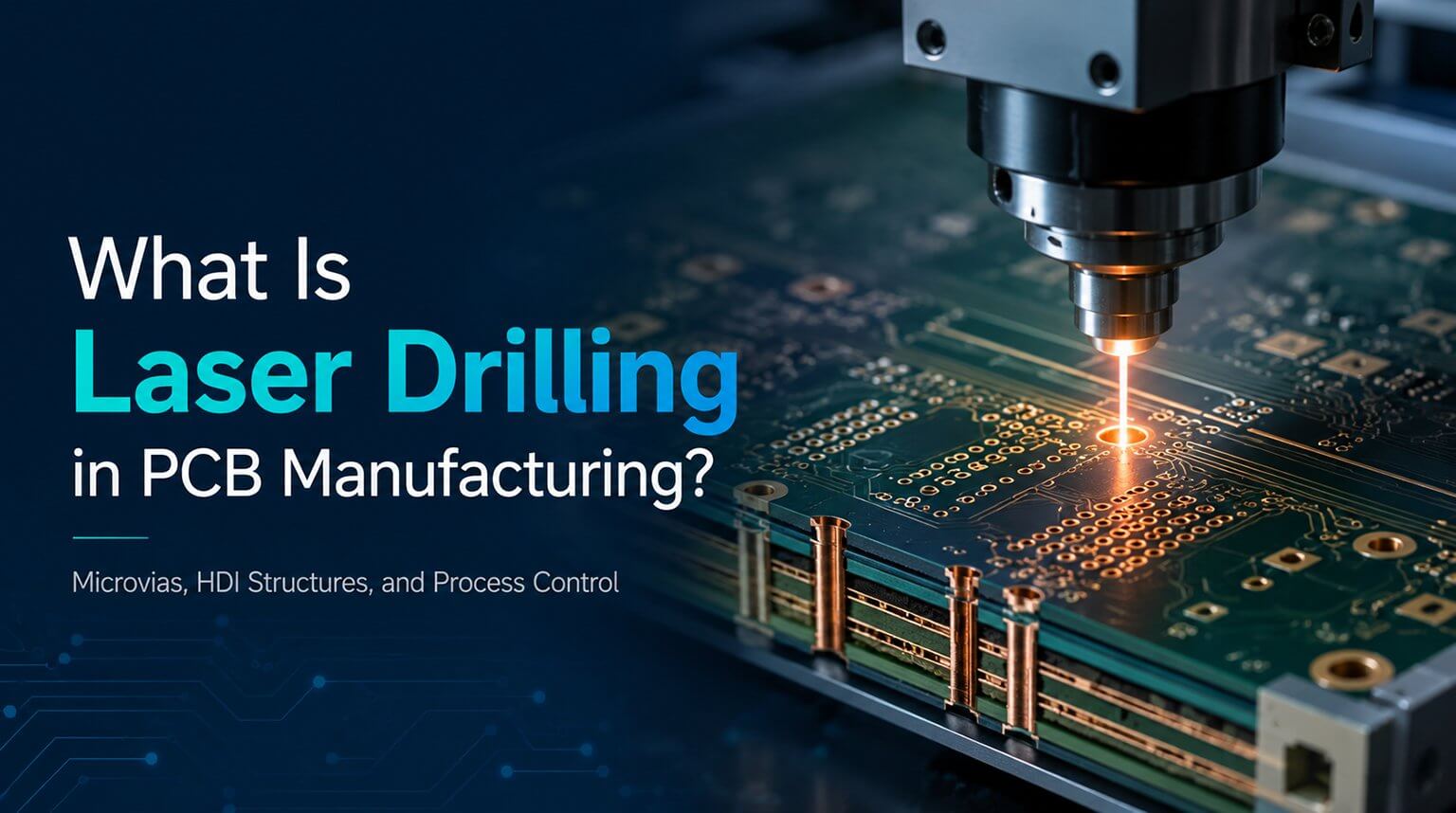
By contrast, HDI PCBs utilize laser drilling technology, reducing minimum via diameters to 0.1 mm or smaller. This enables microvia fabrication, with trace width/spacing commonly controlled at 50 μm, and in advanced applications, down to 20 μm-class ultra-fine circuitry.
This technological breakthrough increases routing density by approximately 3–5× compared to traditional PCBs, allowing substantially more interconnections and functional circuitry within the same footprint.
Example:
In a high-end smartphone mainboard measuring approximately 30 × 70 mm, HDI PCBs can support several thousand to over ten thousand interconnect points, enabling the integration of:
- 5G baseband chips
- Application processors
- High-speed memory
- Camera modules
Under identical area constraints, a conventional PCB typically supports fewer than 2,000 interconnect points, making it insufficient for modern flagship devices.
👉 The dramatic increase in routing density is the primary technical foundation enabling HDI PCBs to replace traditional PCB architectures.
The rapid expansion of 5G communications, AI computing, and high-speed data transmission has significantly elevated requirements for signal integrity.
Traditional PCBs, characterized by wider trace spacing and larger vias, exhibit higher parasitic inductance and capacitance. This often results in signal attenuation, reflection, and crosstalk, particularly in:
- Millimeter-wave frequencies (e.g., 28 GHz)
- High-speed differential signals (tens of Gbps)
HDI PCBs address these challenges through:
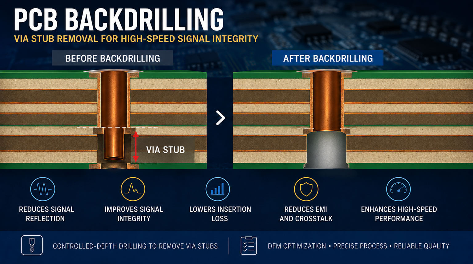
- Micro blind and buried vias, which shorten signal paths
- Low-dielectric-constant materials (Dk ≈ 3.0)
- Ultra-low loss tangent materials (Df ≈ 0.002)
In practical applications, HDI PCBs can achieve:
- 30–40% improvement in signal integrity
- ~30% reduction in transmission loss
Furthermore, multi-layer HDI stack-ups enable precise isolation between power, signal, and ground layers, significantly enhancing electromagnetic compatibility (EMC) and ensuring stable operation in high-performance electronic systems.
HDI PCBs adopt sequential lamination processes, supporting:
- 1+N+1, 2+N+2, and 3+N+3 structures
- Any-Layer HDI architectures, enabling interconnection between any layers
This dramatically increases design flexibility, while also allowing for:
- Ultra-thin substrates (as thin as 0.1 mm)
- Flexible and hybrid rigid-flex configurations
Such capabilities are essential for emerging product forms, including:
- Foldable smartphones
- Wearable devices
- Medical endoscopes
Case in point:
After adopting HDI PCB technology, medical endoscope camera modules have achieved diameters as small as ~3 mm, while failure rates declined significantly. Compared to traditional PCB solutions, overall reliability improved by approximately 50–70%.
👉 This level of process flexibility enables HDI PCBs to meet increasingly diverse and innovative product requirements, further solidifying their role in high-end electronics manufacturing.
Consumer electronics remain the largest application segment for HDI PCBs. Continuous product iteration in:
- Flagship smartphones
- AR/VR devices
- Smartwatches
continues to accelerate HDI demand.
Taking smartphones as an example, the transition from 4G to 5G increased motherboard integration density by approximately 2–3×. As a result:
- Mainstream flagship models typically employ 6-layer or higher HDI structures
- Premium devices increasingly adopt 12-layer Any-Layer HDI designs
According to market data, global demand for HDI PCBs in smart devices reached approximately USD 5.8 billion in 2025, with Any-Layer HDI accounting for 30–35% of the total.
The proliferation of foldable smartphones and wearable devices has further accelerated HDI innovation. Flexible HDI PCBs, characterized by ultra-thin and bendable structures, have achieved over 60% penetration in these applications.
👉 Mass adoption in consumer electronics has transformed HDI PCBs from customized solutions into standardized products—laying a critical market foundation for industry-wide standardization.
The electrification and intelligent transformation of the automotive industry represent a major growth engine for HDI PCBs.
Compared to internal combustion vehicles, new energy vehicles (NEVs) significantly increase PCB value per vehicle due to their reliance on:
- Powertrain electronics (battery, motor, inverter)
- ADAS domain controllers
- In-vehicle infotainment systems
In 2025, China’s NEV passenger vehicle sales reached approximately 15.7 million units, accounting for 55–56% of total vehicle sales. PCB value per NEV is typically 2–3× higher than that of traditional vehicles.
Key technical requirements include:
- 6–8 layer HDI boards for motor control units
- 50/50 μm trace width/spacing for IGBT module substrates
- 16+ layer HDI architectures for L3+ autonomous driving domain controllers
PCB value per unit area in such applications can exceed traditional designs by several orders of magnitude.
Automotive-grade HDI PCBs must also operate reliably across a –40°C to 125°C temperature range, driving higher standards in reliability, process control, and qualification—further accelerating HDI standardization within the industry.
Global digital transformation and the rapid expansion of AI workloads are fueling unprecedented demand for high-layer-count HDI PCBs in data centers and servers.
In 2025, global data center capital expenditure exceeded USD 400 billion, with China accounting for approximately 25%. This has driven HDI PCB demand growth at an estimated 18–22% CAGR.
AI server motherboards are evolving toward 20 layers and beyond, while interfaces such as PCIe 5.0 require transmission losses below 0.3 dB/inch.
The penetration rate of Any-Layer HDI is expected to rise from approximately 32% in 2024 to 50–60% by 2030.
Industry examples include leading global data center operators adopting HDI blind/buried via architectures to:
- Reduce high-speed differential signal crosstalk
- Control dielectric constant variation within ±0.05
- Improve system-level computational efficiency by 20–25%
- Achieve annual failure rates below 0.05%
Mainboards for platforms such as Intel Sapphire Rapids and AMD Genoa now commonly employ 12+ layer HDI designs, further accelerating the standardization of high-layer HDI technology.
In the early stages of HDI development, the technology lacked unified terminology and standards.
In Europe and the United States, it was often referred to as SBU (Sequential Build-Up), while in Japan it was commonly known as MVP (Micro Via Process). The absence of consistent definitions and specifications hindered large-scale industrial adoption.
This situation changed in 1997, when the IPC (Association Connecting Electronics Industries) formally standardized the term “HDI” (High-Density Interconnect) and subsequently released a series of design guidelines, manufacturing specifications, and inspection standards.
Today, the IPC-6012 and IPC-2221 series have become the globally recognized reference standards for HDI PCB design and production. These standards ensure:
- Cross-vendor compatibility
- Interchangeability of products
- Consistent quality and reliability
The establishment of a unified technical framework has provided a solid foundation for HDI PCBs to evolve into an industry-wide standard.
HDI PCB production relies heavily on advanced equipment, including:
- Laser drilling systems
- LDI (Laser Direct Imaging) exposure machines
- High-precision lamination equipment
In the early stages, the high cost and limited availability of such equipment significantly constrained HDI PCB scalability.
In recent years, continuous technological breakthroughs have dramatically improved equipment performance. Modern laser drilling systems now achieve internationally competitive precision, while third-generation LDI systems can control exposure accuracy within ±2 μm.
When combined with AI-driven automated optical inspection (AOI) and defect detection systems, overall production efficiency has increased by approximately 30–40%.
The increasing localization and diversification of core equipment suppliers have:
- Reduced capital investment barriers
- Improved process control stability
- Enabled large-scale mass production of HDI PCBs
This progress has been instrumental in transforming HDI technology from a high-cost specialty solution into a scalable manufacturing standard.
Raw materials play a critical role in determining HDI PCB performance and reliability. As market demand has expanded, the supply chain for high-end materials has matured significantly, including:
- Advanced laminates
- Specialty inks
- High-precision copper foils
Key developments include:
- The penetration rate of modified polyimide (PI) substrates with low dielectric constant and low loss characteristics increased from 18% in 2023 to approximately 28–30% by 2025.
- Domestic suppliers have made substantial progress in specialty inks, with import substitution raising market share from ~9% in 2021 to ~24% in 2025.
- The cost of high-frequency, low-loss laminate materials has declined by approximately 50% compared to 2020.
The combination of improved material performance and declining costs has significantly lowered the overall manufacturing cost of HDI PCBs, enabling their widespread adoption in consumer electronics, automotive electronics, and AI server applications.
Leading PCB manufacturers have achieved notable breakthroughs in HDI process capability through sustained R&D investment. Key milestones include:
- Mass production of 10 μm trace widths, meeting the requirements of autonomous driving GPU substrates and ultra-high-density server boards
- Any-Layer HDI yield rates reaching approximately 85–90%
- Deployment of Industry 4.0 smart manufacturing systems, reducing HDI PCB delivery cycles to as short as 72 hours for rapid-turn projects
The combination of process maturity, higher yields, and shorter lead times has significantly enhanced the competitiveness of HDI PCBs, accelerating their replacement of traditional PCB solutions across multiple industries.
HDI PCBs have become one of the most important growth drivers within the global PCB industry.
Industry data indicates that:
- The global HDI (including SLP) market was approximately USD 9.2 billion in 2018
- It grew to around USD 11.4 billion by 2023
- In 2025, China’s HDI PCB market exceeded RMB 200 billion, with a compound annual growth rate (CAGR) of approximately 20%
- By 2030, the market is projected to approach RMB 850 billion
From a demand structure perspective, AI servers and new energy vehicle electronics are expected to account for nearly 60% of incremental HDI PCB demand, becoming the primary engines of market expansion.
The steady growth in market size reflects widespread industry acceptance and provides strong economic justification for HDI PCBs to serve as a new industry standard.
Historically, the high-end HDI PCB market was dominated by manufacturers in Japan and South Korea. In recent years, leading Chinese PCB companies—such as PCBCool, Shennan Circuits, Wus Printed Circuit, and Kinwong—have achieved significant breakthroughs in advanced HDI technologies through continuous innovation.
As a result:
- China’s HDI PCB localization rate has increased to approximately 40%
- Supply capabilities in consumer electronics, NEVs, and server applications have strengthened substantially
- Chinese manufacturers are increasingly serving not only domestic demand but also global OEMs
This accelerated localization has enhanced China’s influence within the global PCB industry and contributed to the broader international alignment and standardization of HDI PCB technologies.
Government policies have played a pivotal role in guiding HDI PCB industry advancement toward higher value-added segments.
Key policy initiatives include:
- “Made in China 2025”, which identifies high-end PCBs as a strategic development priority
- Over RMB 300 billion in investment directed toward third-generation semiconductors, indirectly stimulating HDI PCB demand
- The 14th Five-Year Plan for Advanced Manufacturing, which targets a 75% import substitution rate for high-end HDI production equipment
- The EU Circular Economy Action Plan for Electronics, mandating 100% halogen-free materials in HDI PCB substrates by 2030
Such policies promote the development of HDI PCBs toward higher density, higher frequency, higher speed, and greener manufacturing, providing strong institutional support for their global standardization.
With its high routing density, superior signal integrity, and unparalleled process flexibility, HDI PCB technology is steadily becoming the new standard in global electronics manufacturing.
Applications span across multiple high-value sectors, including:
- Consumer electronics (flagship smartphones, AR/VR devices, wearable devices)
- New energy vehicles (battery management, ADAS domain controllers, IGBT modules)
- High-performance computing (AI servers, high-speed communication boards)
- Medical and industrial devices (endoscope camera modules, industrial control sensors)
The adoption of HDI PCBs not only expands the functional capabilities of products but also raises technical barriers and market scale, reinforcing their strategic importance.
In this context, selecting a manufacturing partner with mature HDI PCB capabilities and comprehensive engineering support is crucial.
PCBCool offers:
- Advanced HDI production equipment
- A robust and localized supply chain
- Experienced engineering teams capable of full-cycle support, including: PCB design audits, DFM optimization, Rapid prototyping, Mass production
Whether the application involves multi-layer high-density motherboards, flexible or ultra-thin designs, PCBCool provides reliable and efficient manufacturing solutions that help enterprises accelerate time-to-market, reduce development risks, and enhance product competitiveness.