In over 8 years of field support, from Nairobi telecom infrastructure to European industrial IoT deployments, I’ve learned one truth: a well-executed PCB trace repair extends product life, preserves operational continuity, and saves clients thousands in replacement and downtime costs.
Yet, too many “trace repairs” are temporary hacks: globbed solder, dangling wires, or conductive paint that fails within days under thermal cycling or exposure to humidity. True repair is restoration — not just electrical continuity, but also mechanical robustness, thermal stability, signal integrity, and long-term reliability.
This guide reflects methods I use daily in my consultancy, rigorously aligned with IPC-7711/7721C (Rework, Modification, and Repair of Electronic Assemblies, 2024), the global standard for professional electronics repair. Whether you’re recovering a $2,000 control board or salvaging a custom prototype, these techniques ensure the fix lasts — not just works once.
Before picking up your iron, make an informed decision:
| Criterion | Repair Recommended | Replace Recommended |
|---|
| Board Type | Custom, low-volume, legacy, or high-mix (e.g., industrial controllers) | Mass-produced consumer boards (e.g., routers, chargers) |
| Failure Mode | Localized issues: trace break, lifted pad, single component failure | Systemic issues: delamination, via fatigue, widespread corrosion |
| Cost | Repair labor + materials < 15% of board replacement cost | Repair > 15% of replacement cost or > 30% of total system value |
| Reliability Need | Non-safety-critical, indoor, controlled environments | Safety-critical (medical, aerospace), outdoor, high-vibration environments |
Pro Tip: For field-deployed equipment (such as solar inverters in East Africa), repair is often the only option; logistics can make board replacement take weeks.
Based on IPC-7721C Procedure 4.3.2 – “Conductor Repair Using Wire Bond”
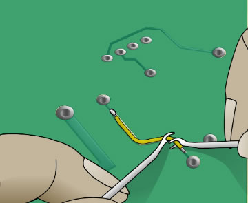
This is the most common trace repair, and the most misapplied. Done poorly, a jumper becomes the next point of failure. Done right, it outperforms the original trace in fatigue resistance and longevity.
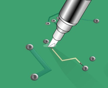
Use a carbide-tip scribe (for example, Xuron 489) – not steel (dulls fast, scratches copper).
Remove solder mask to expose ≥1.5 mm × 1.5 mm bare copper on both sides of the break.
Critical Precaution:
Work at a ≤15° angle to avoid undercutting the copper foil (IPC-6012E allows a maximum undercut of ≤0.05 mm).
Clean with >90% isopropyl alcohol (IPA) and a lint-free wipe (for example, Kimwipe).
Verification:
Use a multimeter in continuity mode. Confirm only the target trace is open — adjacent nets must remain isolated.
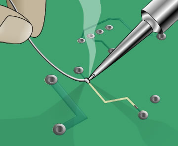
Apply no-clean, rosin-activated flux (for instance, Kester 951 or MG Chemicals 8341) to both pads.
Tin with Sn96.5/Ag3.0/Cu0.5 (SAC305) solder – never use Sn63/Pb37 on RoHS boards (leads to brittle intermetallics and early fatigue failure).
Set iron temperature to 320–340°C (according to IPC-J-STD-001G, Section 5.3 for SAC alloys).
Critical Precaution:
Use minimal solder – aim for a smooth, concave fillet with a 30°–45° wetting angle.
Verification:
Measure resistance – should be <0.1 Ω to adjacent ground plane (if applicable). If higher, oxide remains.
Use solid-core, tinned copper – never stranded (prone to vibration fatigue). Match wire gauge to original trace current capacity, not just width:
Table 1: Solid Wire Equivalents – Current-Matched Selection
(Based on IPC-2221B, Table 6-4, and Thermal Validation, 2025)
| Original Trace Width (1 oz Cu) | Max Continuous Current | Recommended Wire (AWG) | Diameter (mm) | Typical Use Case |
|---|
| 0.2 mm | 0.3 A | 36 AWG | 0.127 | Low-power signals (I²C, UART) |
| 0.3 mm | 0.5 A | 34 AWG | 0.160 | SPI, GPIO |
| 0.5 mm | 0.8 A | 30 AWG | 0.254 | USB D+/D−, sensor power |
| 1.0 mm | 1.5 A | 26 AWG | 0.404 | 5V/12V rails, motor drivers |
Pro Tip: For high-frequency (>10 MHz) or impedance-controlled traces, use micro-coax (such as 36 AWG coax) and terminate the ends properly.
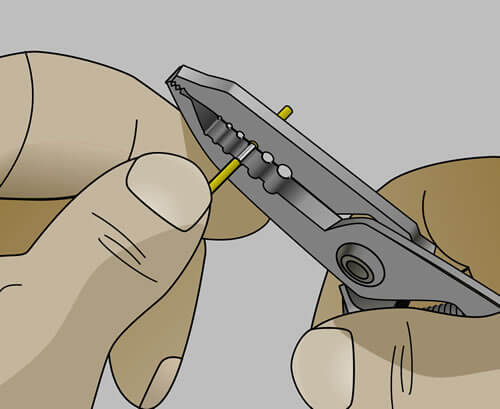
Strip 2.0 mm of insulation using a precision wire stripper (Ideal 45-121) – no nicking.
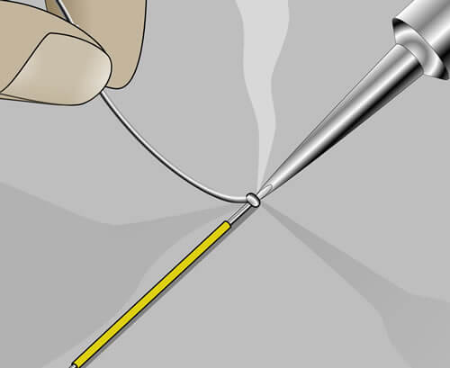
Tin 1.0 mm of each end with SAC305.
Tool Tip: Hold the wire with a third-hand tool or vacuum pickup – never use fingers. Skin oils degrade solderability and can cause dewetting.
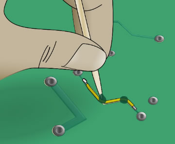
Anchor the first end to the more stable pad (for instance, avoid areas near a connector flex point).
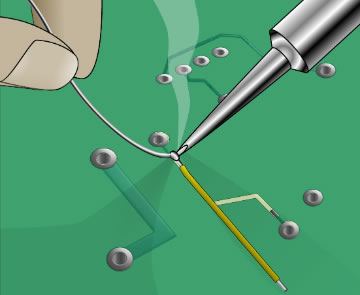
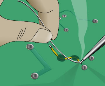
Using the drag soldering method, touch the iron to the pad, feed solder, then gently drag the wire into the molten pool.
Verification:
The fillet must cover ≥75% of the wire circumference and exhibit smooth wetting (IPC-A-610H, Section 8.2.1).
Under a 10x magnifying glass, it was confirmed that there were no voids, solder balls, or mask burns.
Route the wire along the original trace path – never perpendicular (creates a stress riser).
Maintain a ≥0.5 mm clearance from all adjacent traces and components.
High-Density and High-Frequency Note:
For high-density boards, form a gentle “U” loop to absorb thermal expansion (CTE mismatch: FR-4 = 14 ppm/°C; Cu = 17 ppm/°C).
For high-frequency boards, keep wire length < λ/10 at max signal frequency (for instance, <30 mm for 100 MHz).
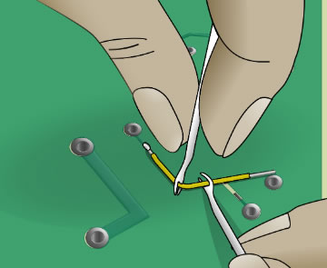
Apply two small dots of UV-curable epoxy (for example, Loctite 3108 or Dymax 9-20502) at the 1/3 and 2/3 points along the wire.
Cure under a 365 nm UV lamp for 30 seconds (or 2 minutes under ambient UV).
Then solder the second end using the same drag technique.
Why not hot glue or silicone?
According to JEDEC JEP182 (2023), they absorb moisture (up to 2% by weight), which can lead to galvanic corrosion in humid environments. UV-curable epoxy remains hermetic.
- Electrical Continuity: <0.05 Ω across the repair (4-wire Kelvin measurement is preferred).
- Isolation Resistance: >1 MΩ to all adjacent nets (use a 50V insulation tester).
- Mechanical Integrity: Gently probe the wire – no movement at the solder joints.
- Visual Inspection: Ensure there is no bridging, lifted pads, or mask damage (IPC-A-610H Class 2 acceptable).
Use 36 AWG micro-coax (for example, the Cooner Wire CW1330).
Terminate with a 22–47 Ω series resistor at the receiver end.
Firmware Validation (ESP32/Arduino):
- Drill a 0.2 mm micro-via beside the pad using a carbide drill bit (max 20,000 RPM).
- Insert a 36 AWG wire and solder both top and bottom.
- Fill with conductive epoxy (for example, EpoTek H20E) and cure for 2 hours at 80°C.
Pro Tip: Avoid silver epoxy – it migrates under bias (IPC-TM-650 2.6.15).
| Method | Why It Fails | IPC Reference |
|---|
| Conductive paint (e.g., CircuitWriter) | Sheet resistivity > 5 Ω/sq; performance degrades rapidly in humid environments | IPC-7721C §5.1.3 — “Not acceptable for permanent repair” |
| Solder blob bridging | High thermal stress leads to micro-cracking within < 72 hours | IPC-A-610H §8.2.5 — “Excessive solder” reject condition |
| Stranded wire jumper | Vibration-induced fatigue causes intermittent opens | IPC-7711C §4.4.1 — “Stranded wire not permitted for conductor repair” |
Before returning the board:
- Electrical: Continuity and isolation verified (4-wire and 50V test)
- Mechanical: Wire strain-relieved, epoxy fully cured, no movement observed
- Thermal: IR scan: ΔT < 5°C at rated current
- Functional: Full system test performed (not just subcircuit)
- Documentation: Photo log and repair report (including time, materials, and validation data)
A PCB board trace repair isn’t complete when the LED turns on. It’s complete when the board survives 5 thermal cycles (−20°C ↔ +70°C), 500 hours of runtime, and a 1-meter drop onto concrete — because that’s the reality your clients face. That’s the standard we uphold. In engineering, reliability isn’t optional; it’s the baseline.
At PCBCool, we bring this same standard to every project. Our engineers don’t just assemble and repair boards — we apply decades of real-world experience to ensure every trace, component, and assembly performs reliably under the toughest conditions. From prototypes to full-scale production, we combine precision manufacturing, expert repairs, and rigorous validation so your electronics just work — every time.