Blog
5 Most Common PCB Defects and How to Prevent Them
Arduino-based prototypes are widely praised for their ease of use and rapid development, but when moving to custom PCBA production, even subtle manufacturing defects can lead to hard-to-diagnose field failures. In our PCB failure analysis lab, we’ve found that over 65% of “mystery” failures in Arduino-derived boards are not caused by code or components, but by layout-induced manufacturing vulnerabilities (IPC Failure Mode Survey, 2024). In this article, we explore the five most common PCB-level failure modes and provide actionable strategies to prevent them before fabrication.
Defect 1: Tombstoning on 0402 Decoupling Capacitors
Symptom: Intermittent MCU resets; the device resumes normal operation after localized reflow.
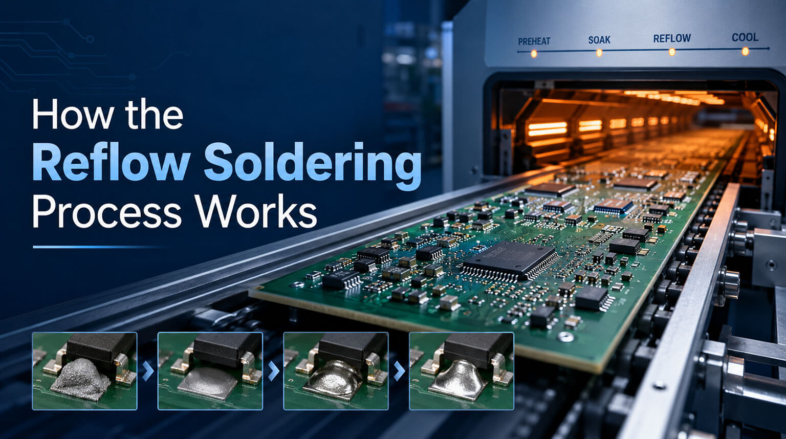
Mechanism: During reflow, asymmetric thermal loading can cause one end of a small capacitor to melt before the other, allowing surface tension to lift the component—resembling a tombstone (IPC-A-610H, Section 8.3.10, 2024). This phenomenon is particularly prevalent with 0402 decoupling capacitors near MCUs (e.g., 100 nF on AVCC), where one pad connects to a large copper pour and the other is attached to a smaller trace.
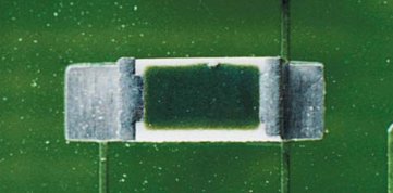
Real-World Example: A client’s ATmega328P-based soil sensor experienced 41% intermittent failures. X-ray inspection revealed that 28% of 0402 decoupling capacitors were tombstoned (Fig. 1). The root cause: Pad 1 was directly connected to a 50 mm² ground pour, while Pad 2 connected to an isolated trace, creating a thermal imbalance.
Prevention Strategies:
- Use symmetric NSMD pads (e.g., 0.6 × 0.7 mm for 0402 components).
- Apply thermal relief to only one pad (single 0.2 mm spoke) to balance heat dissipation.
- Maintain pad copper area ratio ≤ 2:1 to reduce asymmetric heating.
- Specify Type 3 solder paste—smaller particle sizes improve wetting uniformity.

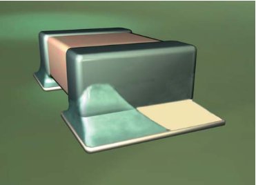
Tombstoned 0402 capacitor, showing classic lift with solder fillet on one end only
Defect 2: Via-in-Pad Voiding Under QFN Thermal Pads
Symptom: Overheating under load; devices trigger thermal shutdown after 10–15 minutes of operation.
Mechanism: Vias located directly under QFN thermal pads (e.g., ESP32-WROOM, AMS1117) can trap flux and moisture during assembly. During reflow, vapor expansion forms voids, which can reduce thermal conductivity by up to 40% (IPC-7095D, Section 5.4.2, 2025). Non-filled vias frequently exhibit >30% void area, significantly impeding heat transfer from the die to the PCB.
Data: Cross-sectional analysis of 120 ESP32 boards revealed:
- Unfilled vias: average void = 37%
- Filled and capped vias (IPC Type VII): average void = 6%
Design Recommendations:
- Avoid vias in thermal pads smaller than 3 × 3 mm whenever possible.
- If vias are necessary (e.g., in a 4-layer stackup), specify filled and capped vias (IPC-4761 Type VII) to minimize void formation.
- Limit via count: ≤8 for a 4 × 4 mm pad, and stagger placement to prevent the “chimney effect.”

X-ray cross-section showing via-in-pad voiding, illustrating how voids impair thermal conduction from the die to the PCB
Defect 3: Solder Bridging on 0.5 mm Pitch TQFPs
Symptom: GPIO pins stuck high or low; USB enumeration failures during device startup.
Mechanism: Excess solder paste on tight-pitch leads (e.g., ATmega328P-AU, 32-pin TQFP) can cause bridging, particularly between pins 15–17 (AVCC/GND/AREF) where thermal mass differs. A standard 0.15 mm stencil thickness is often too thick for 0.5 mm pitch, exacerbating the risk of shorts.
Prevention Strategies:
- Use NSMD (non-solder mask defined) pads to improve paste release and reduce bridging.
- Reduce stencil aperture to ~85% of pad area to limit solder volume.
- Incorporate solder mask webs ≥0.075 mm between adjacent pads.
- Specify Type 4 solder paste (25–36 µm spheres) for fine-pitch components to ensure consistent wetting.

Example of solder bridging on TQFP pins, illustrating how excess paste can connect adjacent leads
Defect 4: Trace Delamination at High-Current Nodes
Symptom: Audible “pop” and burnt smell near high-current areas, such as barrel jacks or motor drivers.
Mechanism: Thin PCB traces (e.g., 0.2 mm) carrying currents >300 mA can overheat, exceeding the FR-4 glass transition temperature (Tg ≈ 135°C). The resin decomposes, causing trace lift-off or delamination (IPC-TM-650 2.4.23, “Thermal Stress Test”).
Design Guidelines (IPC-2221B, Table 6-4):
| Current | 1 oz Copper (10°C Rise) | 1 oz Copper (20°C Rise) |
|---|---|---|
| 500 mA | 0.25 mm | 0.18 mm |
| 1 A | 0.63 mm | 0.45 mm |
Best Practices:
- For 12V barrel jack inputs, use traces ≥0.5 mm wide to handle high current safely.
- Avoid 90° bends near vias, which act as stress concentrators.
- Use thermal reliefs on via barrels (4-spoke, 0.25 mm gaps) to reduce mechanical and thermal stress.
Defect 5: Moisture-Induced Popcorning in BGAs
Symptom: Devices initially function properly but fail after 1–3 weeks in humid environments, such as greenhouse sensors.
Mechanism: Moisture-sensitive devices (MSD Level 3+) (e.g., ESP32-WROVER) absorb ambient humidity. During reflow, rapid steam expansion cracks internal epoxy layers, leading to popcorning failures (JEDEC J-STD-033D, Section 7.3, 2023).
Prevention Protocol:
- Bake MSD Level 3+ parts at 125°C for 24 hours prior to assembly.
- Store components in dry pack (≤10% RH) with humidity indicator cards.
- Limit floor life to ≤168 hours after opening the bag.
- For low-volume builds, consider through-hole components (e.g., ATmega328P-PU, MSD Level 1 – no bake required).

Popcorning failure in a BGA, showing internal delamination after moisture reflow—validates the necessity of bake cycles
Cost of Ignoring PCB Defects
| Defect | Avg. Rework Cost (100 pcs, 4-layer) | Prevention Cost | ROI |
|---|---|---|---|
| Tombstoning | $1,800 (re-spin + labor) | $0 (layout diligence) | ∞ |
| Via voiding | $2,300 (thermal failure / field returns) | $0.15 per unit (filled vias) | 15,000% |
| Bridging | $1,500 (rework station + scrap) | $50 (stencil optimization) | 3,000% |
DFM Checklist for PCB Prototypes
| Check | Tool | Pass Criteria |
|---|---|---|
| Tombstoning risk | Thermal simulation (e.g., Siemens Simcenter) | ΔT < 2.5°C across 0402 pads |
| Via voiding | Cross-section analysis (IPC-TM-650 2.4.22) | Void < 25% of pad area |
| Bridging risk | Paste stencil DRC (e.g., Valor NPI) | Aperture ≤ 85% of pad area |
| Trace current | Saturn PCB Toolkit v9.2 (free) | Temperature rise ≤ 20°C |
| MSD compliance | JEDEC label inspection | Expiry date after assembly date |
Pro Tip: Leverage Your PCB Manufacturer’s Free DFM
Reputable fabs (e.g., PCBCool) provide automated DFM reports during upload. Submitting early can catch issues before production, saving thousands in respins. For mission-critical builds, request:
- AOI (Automated Optical Inspection) for passives
- AXI (Automated X-ray Inspection) for QFN/BGA
- Impedance test coupons for high-speed traces
Final Thoughts
Arduino democratizes functionality, but PCBA production demands discipline. The most elegant code cannot compensate for a layout that ignores the physics of manufacturing. By designing with the process in mind, your boards will ship on time, meet specifications, and stay on budget.
For engineers seeking reliable PCB manufacturing and assembly, PCBCool offers end-to-end solutions—from prototyping to mass production—ensuring your designs perform flawlessly in the field.
Frequently Asked Questions (FAQ)
Tombstoning typically occurs due to asymmetric thermal loading during reflow, where one pad heats faster than the other.
Avoid placing vias directly under QFN thermal pads whenever possible. If necessary, use filled and capped vias (IPC Type VII), limit via count, and stagger via placement to prevent the “chimney effect”.
Solder bridging occurs when excess solder paste and tight lead spacing cause adjacent pins to short.
Ensure traces are wide enough to handle expected current, avoid 90° bends near vias, and use thermal reliefs to reduce localized thermal stress.
Yes. Performing DFM analysis—including thermal simulations, cross-section inspections, and paste stencil checks—identifies potential risks before fabrication, reducing costly respins and field failures.
Absolutely. The principles of thermal balance, paste control, via management, trace sizing, and moisture handling apply to both prototype and volume production PCBs.
George is a certified electrical engineer with experience in PCB design, embedded systems, and IoT hardware development. He works with PCBCool to turn real engineering experience into practical guides for developers and engineers.