Medical PCBA project often gets stuck in 3 options: cost discipline, BOM stability for FDA, and the freedom to iterate on human-factors findings rarely come from the same vendor. EMS shops built for cost protection margin by locking the BOM. Shops built for iteration charge for the engineering bandwidth that lost BOMs require. The FDA’s design control framework asks for both at once.
A US-based medical device CDMO, privately held and PE-backed, with more than 350 completed medical projects on the wall, is moving a 10-channel wearable biosensor charger toward FDA submission. They asked for a quote, then a meeting. They told us cost matters more than turn time. They also told us the BOM has to hold up under FDA scrutiny while their human-factors engineers keep finding things to change. Both at the same time.
The client runs a 12,000 sq ft ISO 13485 facility staffed by a principal engineering team averaging more than 20 years of experience. They design medical devices end-to-end and integrate them. They do not fabricate boards. PCBA assembly is outsourced by design, a deliberate split that keeps their three principal electrical engineers focused on system architecture rather than supplier management.
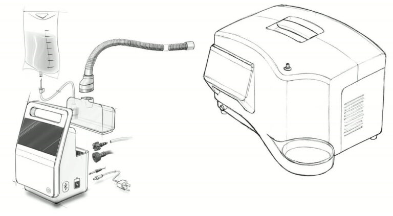
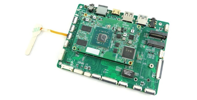
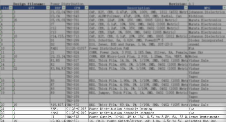
Functionally, the board powers up to ten wearable biosensors at once, with each channel switched independently by its own PMIC.
| Parameter |
Spec |
| Part Number |
01126-01015 Rev 0.1 |
| Dimensions |
190.75 × 112.52 mm (7.51 × 4.43 in) |
| Thickness |
1.57 mm (0.062 in) |
| Layer Count |
2 |
| Substrate |
FR4 Tg180 |
| Surface Finish |
ENIG, per IPC-4552 |
| Copper Weight |
1 oz inner and outer, 35 µm |
| Solder Mask / Silkscreen |
Green / white, top side only |
| Panelization |
Single-out, no array |
| BOM Lines |
24 |
| Component Count |
Approximately 125 |
| Architecture |
10-channel power distribution |
| Quantity Ladder |
100 / 1,000 / 2,000 |
PE ownership pushes unit cost down. The board is a power management subsystem, useful but not differentiating, so it sits squarely in the cost-sensitive category.
FDA 21 CFR Part 820 requires every BOM substitution after design freeze to go through formal change control, traceable to the device history file and device master record. The client said it directly: “stable BOM to meet FDA compliance for medical products.” A supplier that handles substitutions casually is disqualified before the first build.
And IEC 62366-1 Clause 5.7 formative usability evaluations keep surfacing issues — connector alignment, indicator visibility, casing temperature — that loop back to the PCBA. Two to five revision cycles between EVT and DVT lock is realistic for this product class. A supplier that cannot turn protos quickly, hold component-level traceability across revisions, and feed clean ECO documentation back into the client’s DHF will quietly break the FDA timeline.
The villain is not a single weak link. It is the gap between mass-EMS economics and medical standards, which by regulation requires both repetition and disciplined change. Most suppliers pick a side. This program needs both.
We flew from Shenzhen to Colorado before quoting a single tooling fee. Two days of travel — across the Pacific, through Denver, and south to the client’s facility.
Scott met us at the door and walked us straight to the bench where the biosensor charging cradle sat. He explained how the ten-channel architecture had evolved after their latest usability study, and why the Rev 0.1 BOM was already provisional. That single conversation surfaced more engineering context than three months of email could have.
We had a meeting. The discussion stayed practical: cost structure, BOM change-control workflow, which components they wanted us to procure and which specialty parts they would ship from their own stock. We walked through our Shenzhen, Malaysia, and Mexico production options; they walked us through their DHF templates and explained exactly how change records needed to flow back for FDA compliance.
Two engineering teams working through the same BOM with a whiteboard between them. By the end of the day the scope was agreed: turnkey PCBA with full procurement, flying-probe and electrical testing on our side, so their three principal engineers could stay on system design instead of chasing suppliers.
It was a good meeting. Both sides left with the same checklist.
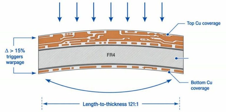
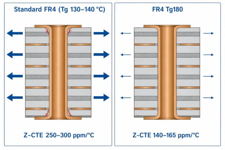
A two-layer build without an inner copper plane has nothing to constrain the layers if their copper coverage is uneven. The PCBCool DFM protocol holds top-to-bottom copper coverage within ±15 % and tunes the lamination cycle for the Tg180 resin system, which is harder to drill than standard FR4 and chews through bits roughly 15–20 % faster.
The board structure is visible from the BOM. One PMIC, one output, one enable line, replicated ten times. That topology pushes layout review beyond standard SI checks: thermal isolation between adjacent PMICs and ground coupling through shared returns both have to be verified before the first build.
The original Rev 0.1 BOM substituted Murata NFM21PC104 for thirteen X2Y feedthrough capacitors at C1, C2, and C14–C41. NFM21PC104 is a feedthrough capacitor. It is not an X2Y type. The two are not interchangeable; their balanced-capacitance behaviour and EMI characteristics differ enough that swapping one for the other quietly breaks the filtering the part exists to provide. A pre-production BOM review caught the substitution and proposed Yageo CX0805MRX7R7BB104 as the correct X2Y equivalent.
Worth asking whether your current supplier would have caught that before first article, or after.
The board carries multi-ampere load through a TPSM843620SITR rated to 6 A at 4–18 V input, so the substrate sees real thermal cycling in service. The CTE difference is not academic. It is the gap between via barrels that survive the device’s service life and via barrels that crack in the field.
Material cost runs 25–40 % over standard FR4, paid back across the warranty period rather than the BOM line.
Black pad is the failure mode that destroys medical-device fielded-life claims. The IPC spec exists because suppliers who don’t control phosphorus to the right window produce boards that solder fine on the line and fail in service.
Three standards do most of the work on this program. A fourth governs the change-control workflow that keeps everything traceable.
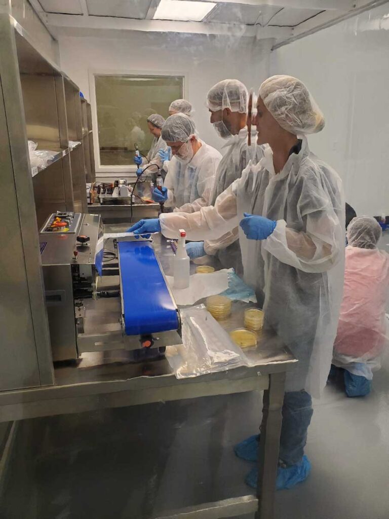
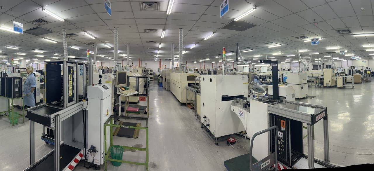
PCBCool holds ISO 9001, ISO 14001, ISO 13485, UL, RoHS, and REACH certifications across two Shenzhen facilities founded in 2008, with additional capacity in Malaysia and Mexico for nearshoring or trade-compliance purposes. In any plant, we apply the consent and strick QC SOP.
ECO handling is the part that makes or breaks medical supplier relationships. FDA 21 CFR 820.30(i) requires every design change to be evaluated against validation status. Every BOM revision generates a documented change record cross-referenced to the client’s DHF and DMR entries, with traceability logs updated in step. Connector swaps, indicator changes, thermal layout adjustments — handled as routine change events, not exceptions. The full workflow is available for the client’s audit team ahead of formal qualification, on request.
The program cleared sample acceptance and EVT without issues. Production has since ramped through the 1000-unit milestone and is running sustained batches toward the high volume. The RT9728BHGE buffer stock that was pre-positioned during Phase 0 has already absorbed two Richtek lead-time slips without interrupting the build schedule. BOM revision control — the concern the client raised in our very first conversation — has held through three ECOs, each documented, cross-referenced to the DHF, and closed within the agreed review window.