Printed Circuit Boards (PCBs) are so pervasive in our life; it is easy to underestimate them. On the surface, a PCB looks like a simple green board with copper lines, a few drilled holes, and some tiny components sitting neatly in place. But anyone who has spent time around board design or fabrication knows the reality is very different. A PCB is not just a carrier for components; it is the physical structure that makes the entire electronic system possible. It has to support the circuit mechanically, connect it electrically, survive heat and vibration, and still behave exactly as the designer intended.
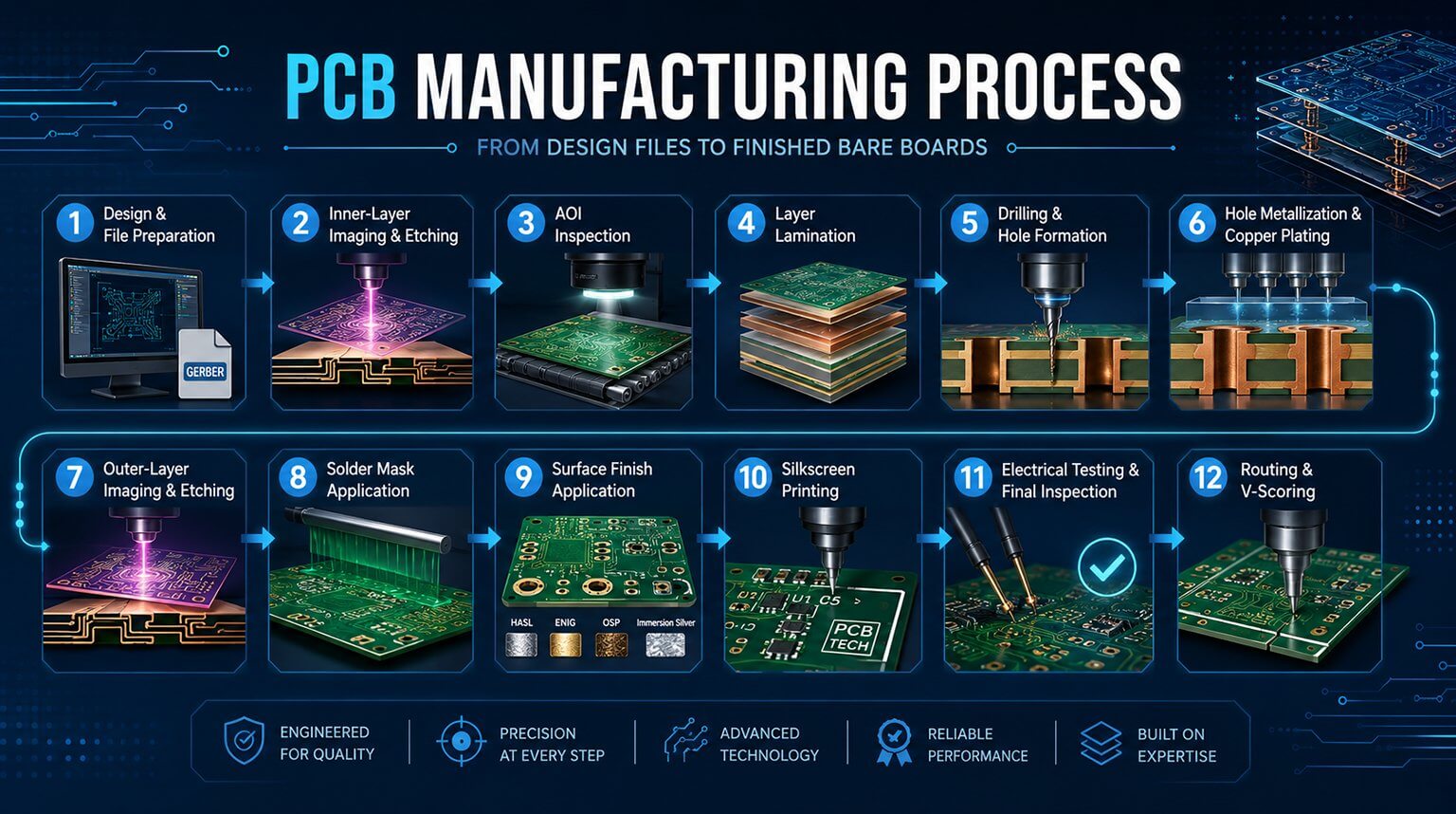
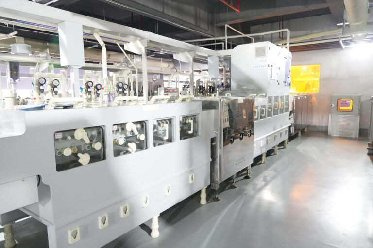
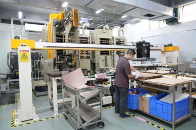
That is why PCB manufacturing is one of the most fascinating parts of electronics. It sits at the point where digital design meets chemistry, precision drilling, imaging, plating, inspection, and a surprising amount of process discipline. A design may begin as a neat schematic on a laptop, but turning it into a reliable physical board takes many carefully controlled steps. In modern fabrication, even a small mistake in layer alignment, copper thickness, drilling accuracy, or surface finish can affect the final performance of the board.
This article follows the general process for standard bare PCB manufacturing and includes practical points drawn from PCBCool’s own production experience. Special board types, such as flexible PCB and metal-core PCB, may require additional process controls and are not covered in detail here.
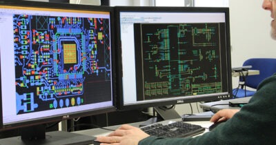
PCB design begins in CAD software, where the circuit schematic is laid out and a “blueprint” is created. In this step, engineers convert circuit requirements into a physical layout using EDA (Electronic Design Automation) tools such as Altium Designer, Cadence Allegro, KiCad, or Siemens Xpedition.
At this stage, the schematic is translated into a board layout that defines component placement, routing paths, power distribution networks, grounding strategy, impedance-controlled traces, and layer stack-up. A good layout is not only electrically correct; it must also be practical to build.
Before fabrication begins, the design undergoes DFM (Design for Manufacturability) checks. Fabricators review trace widths, clearances, drill sizes, annular rings, solder mask openings, copper-to-edge spacing, and other parameters to ensure the board can be manufactured reliably. For high-speed boards, signal integrity and power integrity checks are often part of this stage as well. These checks help prevent expensive surprises after fabrication has started.
Once approved, the design is exported into Gerber files, drill files, and fabrication drawings. These files become the blueprint for production. In many fabrication facilities, Computer-Aided Manufacturing (CAM) engineers perform a final review of these files before production begins, ensuring that the design data is complete, manufacturable, and ready to move onto the shop floor.
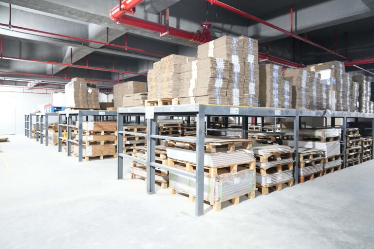
After the project is confirmed and the production files have been reviewed, the manufacturer prepares and pre-treats the base materials required for the PCB.
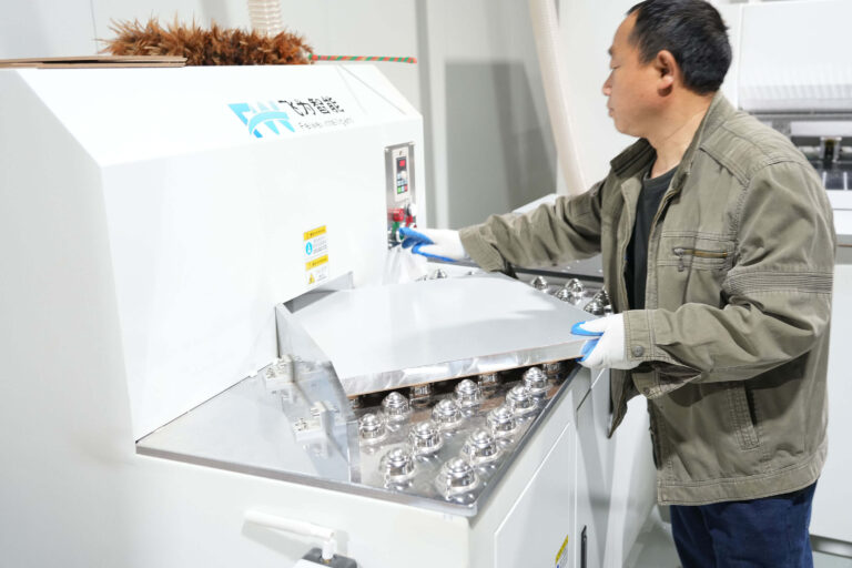
Large copper-clad sheets are first cut into production panel sizes using a cutting machine. The panels are sent through a brushing and cleaning machine to remove surface oxidation, dust, oil, and other contaminants.
This process ensures that the panels are suitable for the equipment and processes that follow. It also creates a cleaner and more stable copper surface, which helps improve dry film adhesion during inner-layer imaging.
With the design files finalized, the manufacturing process moves to the first stage where the actual circuit pattern begins to take shape. For multilayer PCBs, fabrication typically starts with the inner copper layers that will eventually be buried deep inside the finished board.
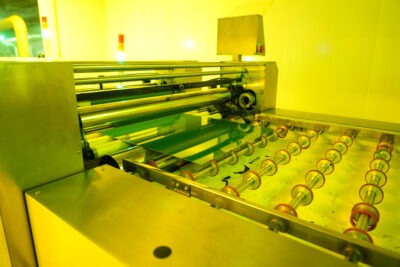
The process begins with copper-clad laminate sheets coated with photoresist. Using Laser Direct Imaging (LDI), the desired circuit pattern is transferred onto the panel. The exposed photoresist hardens while the remaining resist is removed during development. Chemical etching then removes unwanted copper and leaves behind the intended traces and copper features.
This is the stage where the first physical representation of the circuit is created. If the imaging or etching is off, the problem will follow the board through the rest of the process. That is why cleanliness, alignment, and exposure control matter so much here. A small amount of contamination or a slight exposure error can change the trace shape enough to affect later stages.
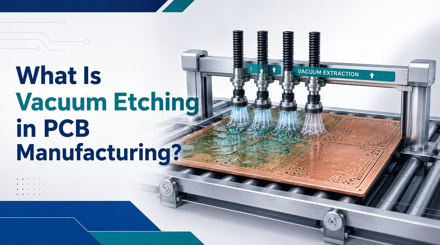
As trace and spacing requirements become finer, the etching process also becomes harder to control. For very fine-line designs, PCBCool may use vacuum etching to improve process stability, especially for 3/3 mil trace and space requirements or finer. We cover this topic separately in our article: What Is Vacuum Etching in PCB Manufacturing
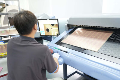
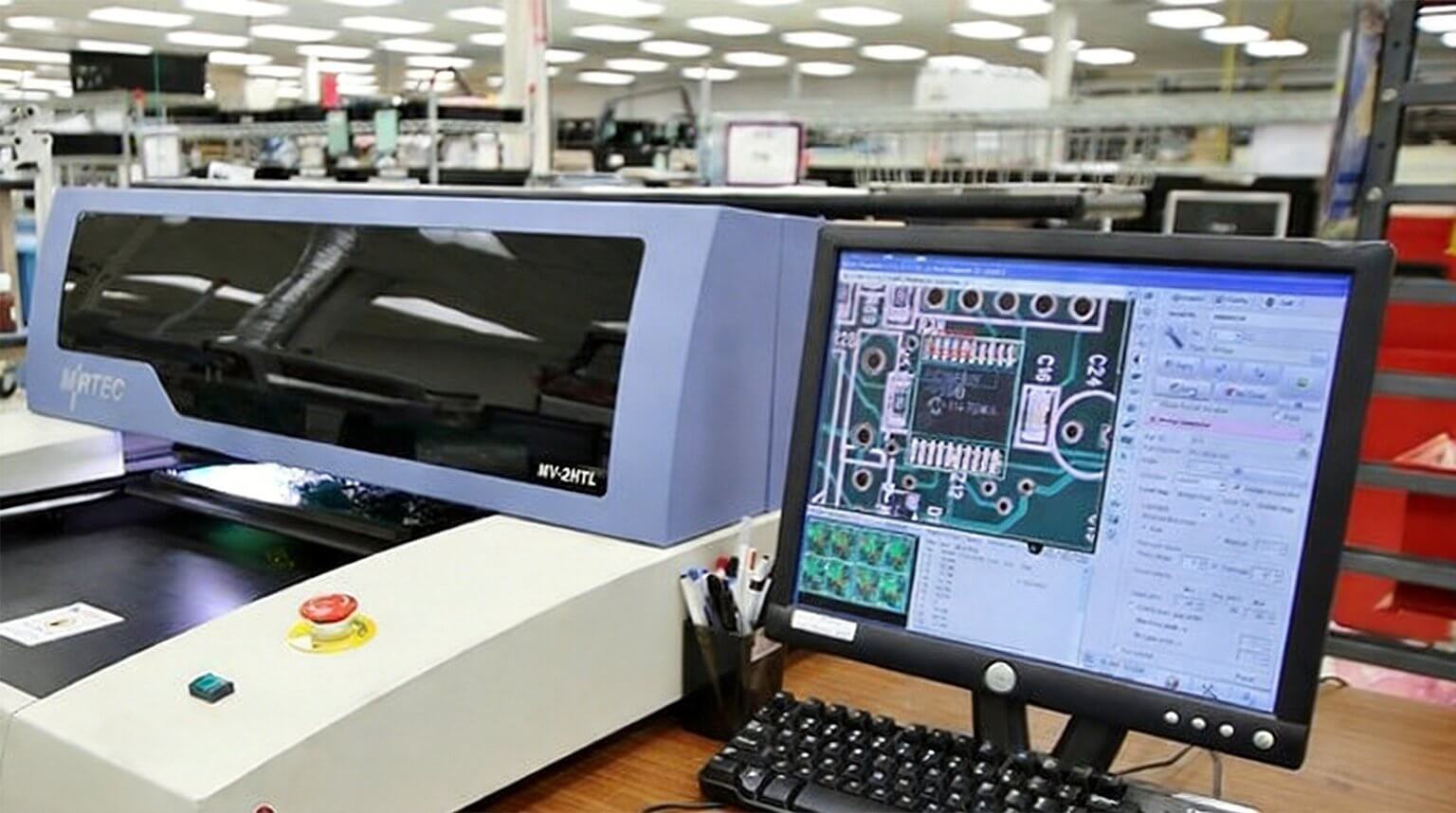
Before the inner layers are buried inside the PCB, they undergo AOI (Automated Optical Inspection). AOI systems use high-resolution cameras and image-processing software to compare the manufactured pattern against the original design data.
The system looks for opens, shorts, missing copper, under-etched areas, and other defects. Since these layers will soon become inaccessible, AOI acts as a critical quality checkpoint. Catching a flaw here is far easier than discovering it after lamination, when the defect is trapped inside the finished board.
By identifying defects early, manufacturers can reject faulty panels before additional time, materials, and processing costs are invested in them. This not only improves production yield but also helps ensure that only defect-free layers move forward to the next stage of fabrication.
After inspection, the inner layers are prepared for lamination. Target holes are made to help align the layers accurately during stacking, and the copper surfaces are treated to improve bonding with the prepreg resin.
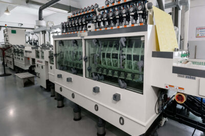
The individual layers are then stacked together according to the PCB stack-up design. Sheets of prepreg, a fiberglass material impregnated with partially cured epoxy resin, are placed between the copper layers. The stack is then subjected to controlled heat and pressure inside a laminating press.
During this process, the epoxy flows and bonds the layers into a single rigid structure. Lamination is one of the most important stages in PCB fabrication because poor control can lead to voids, shifting, resin imbalance, or long-term reliability problems. The board has to survive temperature changes, assembly heat, and years of use, so the bond between layers must be solid.
If the lamination is done well, the PCB comes out as one unified multilayer structure with the internal layers locked in place. From this point onward, the board is no longer a stack of separate sheets; it is a single structure.
The laminated board now requires holes for vias, component leads, mounting points, and other features. CNC (Computer Numerical Control) drilling machines create these holes with high precision, often drilling thousands of holes in a single panel.
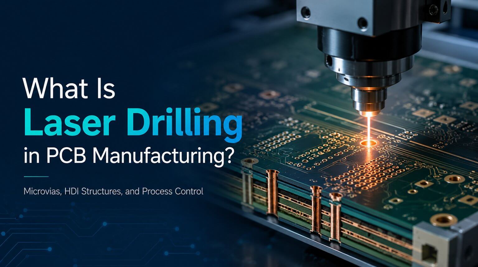
Modern multilayer boards may also use X-ray or optical alignment systems to ensure the drill targets match the internal copper layers accurately. For high-density interconnect designs, laser drilling is commonly used to create microvias that are much smaller than conventionally drilled holes. These tiny holes are essential when designers need more routing in a smaller area.
After drilling, the panels undergo cleaning and desmear processes to remove debris and prepare the holes for metallization. This matters because the next stage depends on clean hole walls. If resin smear or drilling residue remains, the copper plating may not bond properly.
At this stage, the drilled holes are still electrically non-conductive. To create electrical connections between layers, the hole walls must be coated with copper.
The process begins with electroless copper deposition, which forms a thin conductive layer on the hole walls and panel surfaces. The board then undergoes electrolytic copper plating, where additional copper is deposited using electrical current. This plating forms the via barrels that connect different layers of the PCB.
Consistent plating thickness is essential because thin or uneven copper can create long-term reliability problems, especially in applications exposed to thermal cycling and mechanical stress. A via that looks fine on the outside can still fail later if the copper wall inside the hole is too weak. That is why manufacturers closely monitor current density, chemistry, and panel geometry during plating.
Once the vias are plated, the outer copper surfaces are patterned using a process similar to the inner layers. A photoresist is applied, exposed using LDI, and developed to define the desired circuitry.
Chemical etching removes unwanted copper while preserving the protected regions. This creates the visible traces, pads, and copper features that will eventually interface with electronic components. By the end of this stage, the board begins to resemble the familiar PCB seen inside electronic products.
This step is especially important for assembly quality. Outer-layer features must be accurate because they directly affect soldering, connector fit, and signal behavior. On fine-pitch designs, even a small variation can create a problem later during assembly.
At this stage, the PCB’s copper circuitry is fully formed, but the board is still far from ready for assembly. The exposed copper circuitry must be protected from oxidation, contamination, and accidental short circuits. To accomplish this, manufacturers apply a solder mask across the PCB surface.
A liquid photoimageable solder mask is applied and then selectively exposed so that only component pads, test points, and plated holes remain uncovered. The hardened solder mask protects the copper while helping prevent solder bridges during assembly.
Even with solder mask protection, exposed copper pads can oxidize over time. To preserve solderability, manufacturers apply a surface finish to all exposed copper areas.
Common finishes include HASL (Hot Air Solder Leveling), ENIG (Electroless Nickel Immersion Gold), and OSP (Organic Solderability Preservative). Each offers different advantages in terms of cost, flatness, shelf life, and assembly performance. HASL is widely used and economical, ENIG is popular for flatness and fine-pitch work, and OSP is often chosen when cost and simplicity matter.
The choice depends on component density, reliability requirements, and manufacturing budget. In practice, surface finish is not just a final touch. It is one of the decisions that shapes how easily the board can be assembled and how well it will age before assembly.
At this point, the PCB is electrically complete and almost ready for assembly. The copper circuitry has been formed, protected by solder mask, and finished with a surface coating to ensure reliable soldering. However, one final layer of information still needs to be added before the board can move toward testing and production: the silkscreen.
The silkscreen layer contains reference designators, polarity markings, logos, revision numbers, and other information that helps with assembly and maintenance.
Manufacturers typically apply white ink using screen printing or direct inkjet printing techniques. The markings are then cured to create a durable identification layer. Although silkscreen does not affect electrical performance, it improves assembly efficiency, troubleshooting, and long-term serviceability. Good silkscreen design helps technicians orient parts correctly, identify test points quickly, and avoid mistakes during manual inspection. When a board enters production or rework, clear markings save a great deal of time.
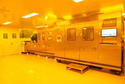
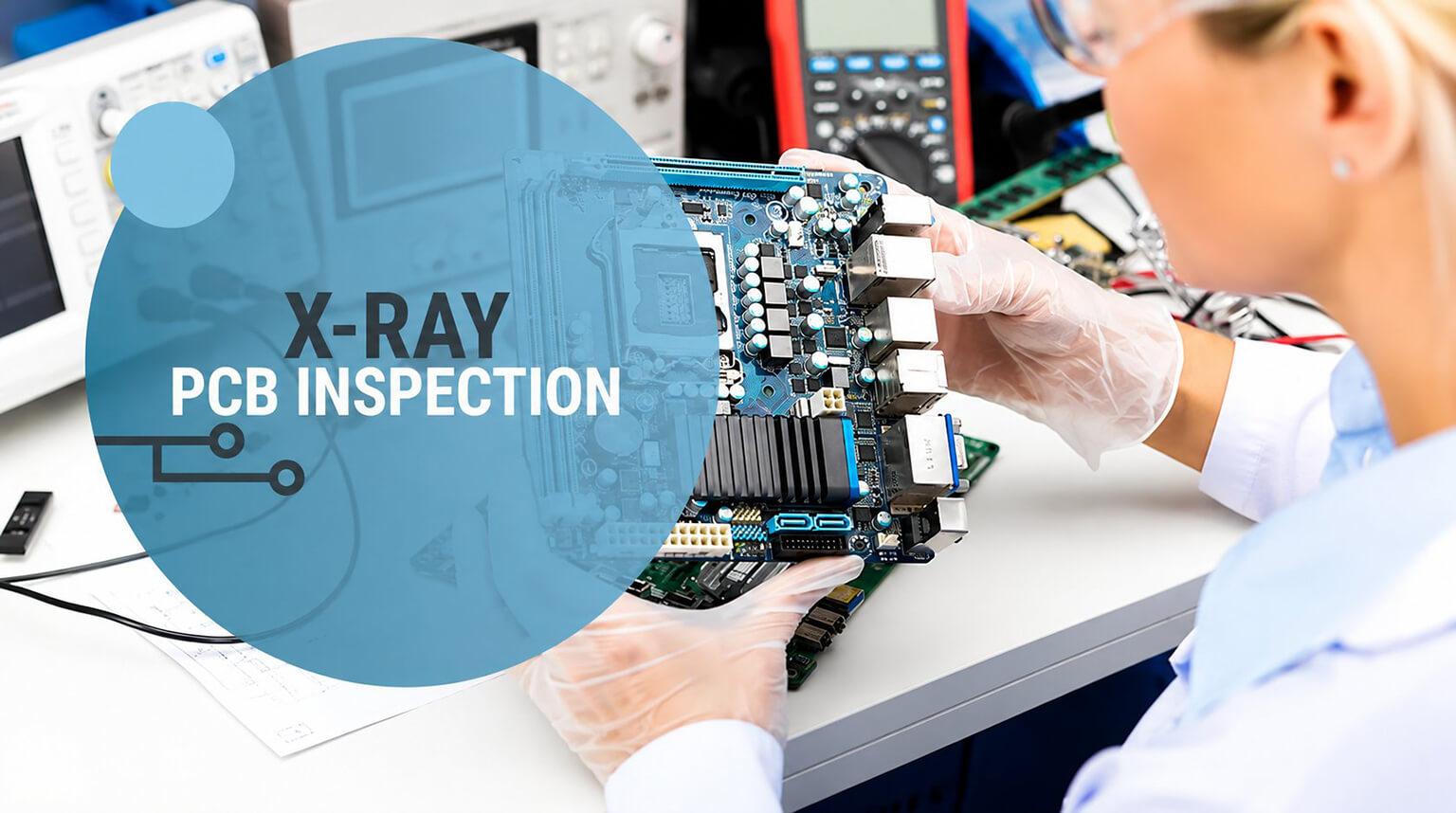
Before the PCB is approved for shipment, it must pass electrical testing and inspection. Electrical testing verifies that all intended connections exist and that no unintended shorts are present. Prototype boards are often tested using flying-probe systems, while high-volume production commonly uses bed-of-nails fixtures for faster throughput. The board also undergoes visual inspection, often with AOI systems, to detect defects such as missing copper, solder mask issues, or dimensional inaccuracies.
This is the final proof that the board is ready for the next stage. A PCB can look perfect and still fail electrically, so testing protects both the manufacturer and the customer. Only boards that meet all quality requirements proceed to the final stage.
Throughout fabrication, multiple PCBs are typically processed together on a larger production panel. The final manufacturing step is separating the individual boards from this panel.
Manufacturers generally use either routing or V-scoring. Routing uses CNC cutting tools to follow the board outline, while V-scoring creates controlled grooves that allow boards to be snapped apart easily. After depanelization, the boards undergo a final inspection and are prepared for shipment.
This step is mechanical, but it still needs care. Poor depanelization can leave burrs, stress the board edge, or damage nearby features. A clean separation is the last sign that the fabrication process was controlled well from start to finish.
After depanelization, the finished PCBs are then packaged and prepared for shipment to the assembly facility, where electronic components will be mounted and soldered onto the board.
With this final step complete, the PCB fabrication process officially comes to an end. What began as a digital design file has now been transformed into a fully manufactured bare circuit board, ready to serve as the foundation of an electronic product.
Modern PCB manufacturers employ extensive quality-control systems throughout fabrication. Chemical baths, temperatures, plating parameters, dimensional tolerances, and inspection results are monitored not as separate tasks, but as part of the same goal: keeping the board accurate, stable, and reliable enough to meet Class 2 or Class 3 requirements.
This also explains why the PCB manufacturing process is difficult to describe completely in one article. In real production, a complex multilayer PCB may undergo more than 20 processing steps from raw laminate to finished board, with inspection and process control built into many of those stages.
Although the technologies used in fabrication continue to evolve, the underlying goal remains unchanged: create accurate, durable, and dependable interconnections for modern electronics.
The next time you look at a PCB, it is worth remembering that behind its seemingly simple appearance lies a remarkable combination of engineering, materials science, and manufacturing precision.
If you have PCB manufacturing needs, partnering with PCBCool gives you access to 1–40 layer bare PCB fabrication, PCBA assembly, and box build integration, helping move your project from concept to finished product.