Blog
What Is PCB X-Ray Inspection and Why Is It Needed?
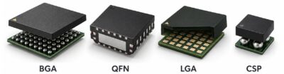
As PCB assemblies become smaller, thinner, and more densely packed, more solder joints are no longer visible after assembly. Components such as BGAs, QFNs, LGAs, and other bottom-terminated packages place their electrical connections underneath the component body, where manual inspection and AOI cannot directly see them.
This is where PCB X-ray inspection becomes important. Instead of only checking the surface of the board, X-ray inspection allows manufacturers to look through the component and PCB structure to evaluate hidden solder joints and internal assembly quality.
If you are not yet familiar with PCB X-ray inspection, this article is a good place to start. We will walk through the technology in a practical way, so you can understand what it does, where it is useful, and why it has become an important part of modern PCB assembly quality control.
What Is X-Ray Inspection in the PCB Industry
For people outside the electronics industry, the word “X-ray” may first bring medical imaging to mind. PCB X-ray inspection is based on a similar physical principle, but its purpose is different. It is used to examine the internal condition of a bare PCB or an assembled circuit board without cutting into the board.
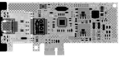
During inspection, X-rays pass through the PCB. Different materials absorb the radiation at different levels. Dense materials such as copper, solder, and component leads absorb more X-rays and appear darker or more defined in the image, while less dense materials allow more radiation to pass through.
This contrast allows the inspection system to reveal details that cannot be checked from the surface, including solder joints under components, vias, and structures inside multilayer boards.
Because the board remains intact, X-ray inspection is considered a non-destructive inspection method. In PCB assembly, it is commonly used after soldering to check hidden connection areas before functional testing, failure analysis, rework decisions, or final quality review.
PCB X-ray inspection systems are usually divided into three types: 2D, 2.5D, and 3D.
- 2D X-ray inspection provides a flat image of the inspected area.
- 2.5D X-ray inspection adds angled-view observation.
- 3D X-ray, also known as CT X-ray inspection, can reconstruct a three-dimensional image through multi-angle scanning.
Among these methods, 3D X-ray provides the most detailed view of internal structures, but it also requires higher equipment investment, longer inspection time, and more complex operation. For this reason, 2D X-ray remains the most commonly adopted method in everyday PCB assembly production, while 3D X-ray is usually reserved for more advanced inspection needs.
Why X-Ray Inspection Matters in Modern Electronics Manufacturing
The need for X-ray inspection comes from a clear industry trend: electronic devices are becoming smaller, lighter, and more functionally dense.
To support this trend, component packaging has evolved from traditional through-hole parts to surface mount devices, and then to more advanced packages such as BGA, QFN, LGA, and CSP. These packages save PCB space and support higher performance, but they also create a new inspection challenge.
In many of these components, the solder joints are located underneath the package body. After placement and reflow soldering, those joints are no longer visible from the surface.
A BGA package, for example, may contain hundreds or even thousands of solder balls under the component. A board can pass visual inspection and AOI while still having hidden defects under the BGA. The same problem can occur with QFN packages, especially around thermal pads and bottom-side soldering areas.
X-ray inspection helps manufacturers reduce this blind spot. It allows engineers to inspect hidden solder joints before the board moves into later testing stages, rework, shipment, or product integration.
This is especially important for projects involving:
- Fine-pitch BGA components
- High-density SMT assembly
- QFN packages with thermal pads
- First Article Inspection before mass production
- Failure analysis for PCB or PCBA issues
In these cases, X-ray inspection is not just an additional quality step. It is a practical way to confirm whether hidden solder joints have formed correctly.
PCB Issues Detectable by X-Ray Inspection
BGA Solder Voids
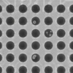
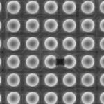
In a BGA solder ball, voids usually appear as lighter spots inside the darker solder area. Engineers check three points: how large the voids are, where they are located, and whether they are isolated or repeated across many balls.
Small scattered voids may be acceptable, but large voids, concentrated voids, or repeated voiding patterns can suggest process issues such as trapped gas, poor paste release, or an unsuitable reflow profile.
Hidden Solder Bridges
A hidden solder bridge usually appears as a dark connection between two solder areas that should be separate. In BGA inspection, the key is to check whether each solder ball keeps a clear gap from the next one.
If two balls look merged, stretched, or connected by a narrow solder path, the board may have a short-circuit risk. This is why X-ray is often used before powering boards with dense bottom-side connections.
Misaligned BGA Balls or Component Shift
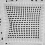
For BGA alignment, engineers look at the overall ball pattern. A normal array should show even spacing, consistent ball shape, and a regular grid.
If the package has shifted, the image may show offset balls, uneven spacing, compressed joints on one side, or stretched joints on the other. This helps confirm whether the component stayed aligned during placement and reflow.
QFN Thermal Pad Voiding
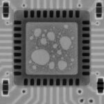
For QFN packages, X-ray is mainly used to check solder coverage under the exposed thermal pad. Voids appear as lighter areas within the soldered pad region.
Engineers usually look at the total void area, the largest individual voids, and whether voids are concentrated in the heat-transfer path. If the thermal pad shows poor solder spread or excessive voiding, the process may need adjustment in stencil design, solder paste volume, or reflow settings.
Solder Ball Wicking
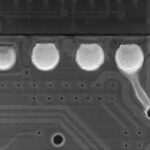
Solder ball wicking means solder has moved away from the intended joint area. In an X-ray image, it may show as reduced solder volume at the joint, an uneven ball shape, or an abnormal solder trace extending toward a via or nearby structure.
The key difference from voiding is that voiding is empty space inside the solder, while wicking shows solder flowing away from where it should remain.
AOI vs X-Ray Inspection vs Functional Testing
| Method | Main Purpose | Best For | Limitation |
|---|---|---|---|
| Visual Inspection | Basic surface review | Obvious appearance defects, manual quality checks | Cannot detect hidden solder joints |
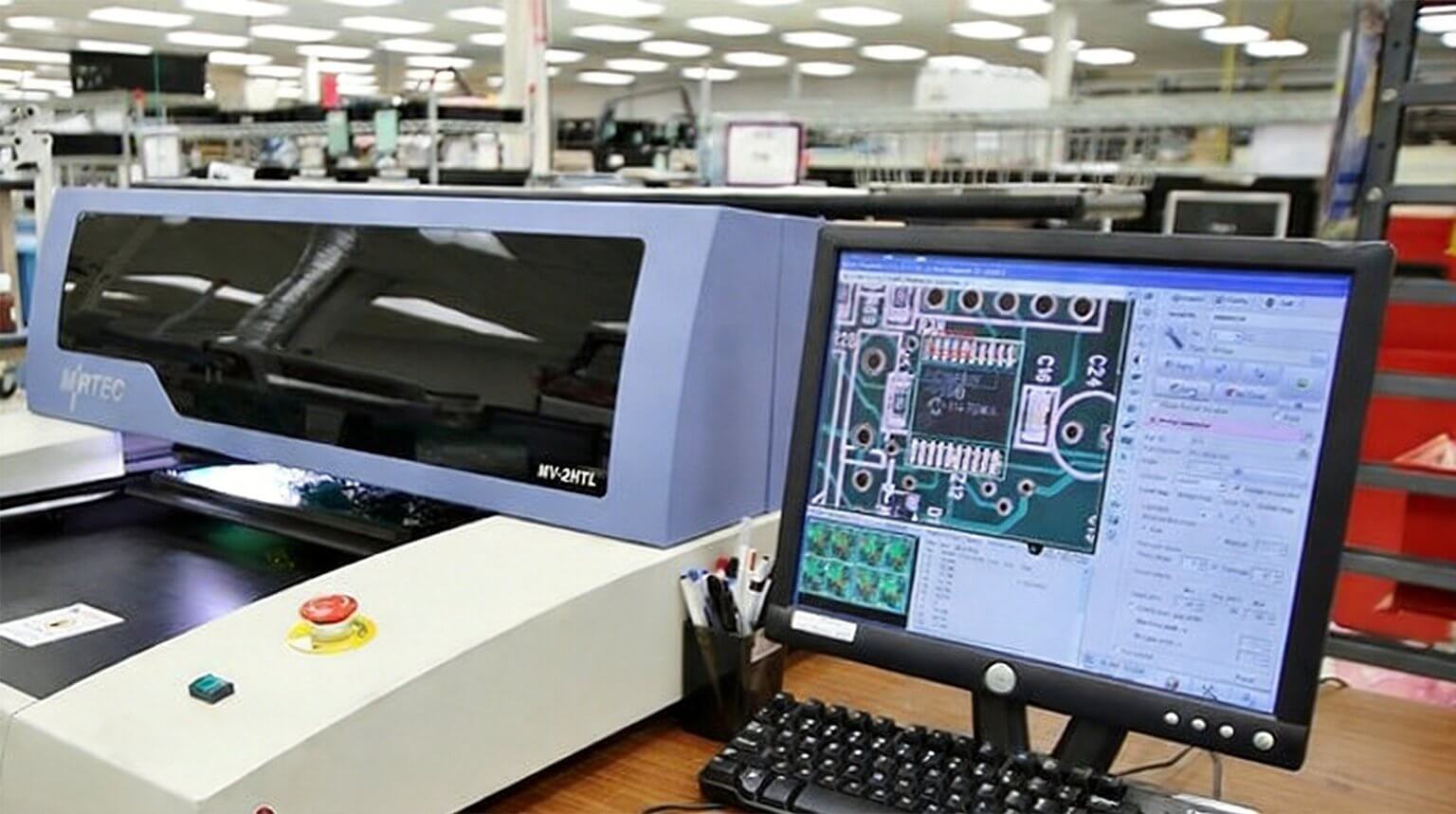
| AOI | Automated optical inspection | Component placement, polarity, missing parts, visible solder defects | Cannot see underneath BGA, QFN, CSP, or other hidden packages |
| X-Ray Inspection | Hidden solder and internal inspection | BGA, QFN, CSP, solder voids, hidden bridges, insufficient solder, internal defects | Cannot fully verify product function |
| ICT | Electrical in-circuit testing | Shorts, opens, wrong values, missing components, basic circuit-level faults | Requires test points and fixtures |
| FCT | Functional performance testing | Verifying whether the assembled board works as intended | May not identify the physical root cause of a defect |
Does Every PCB Assembly Need X-Ray Inspection
No. X-ray inspection is not necessary for every PCB assembly.
For simple boards with mostly visible solder joints, AOI, visual inspection, ICT, and functional testing may be enough. For example, a board using standard resistors, capacitors, diodes, SOIC packages, connectors, and through-hole components may not need X-ray inspection unless there is a specific quality concern.
X-ray inspection becomes more valuable when the assembly includes:
- Hidden solder joints
- BGA or QFN packages
- High-density SMT areas
- Fine-pitch components
- Thermal pad soldering
- High-reliability application requirements
- Failure analysis needs
In practical PCBA manufacturing, the question should not be, “Does every board need X-ray inspection?”
A better question is:
Where are the hidden risks in this assembly, and which inspection method can detect them?
If the main risk is visible soldering quality, AOI may be the right method. If the risk is hidden under a BGA or QFN package, X-ray inspection becomes much more important. If the concern is final product performance, functional testing is required.
A capable PCBA manufacturer should recommend the right inspection plan based on the actual board design, component package, application environment, and customer quality requirements.
What to Look for in a PCBA Manufacturer with X-Ray Inspection Capability
When choosing a PCBA manufacturer, it is not enough to ask whether the factory has an X-ray machine. The more important question is whether the team knows when and how to use it correctly.
A capable manufacturer should understand:
- Which component packages require X-ray inspection
- How to evaluate BGA solder joint quality
- How to identify solder voids, bridges, opens, and misalignment
- How to inspect QFN thermal pad voiding
- How to connect X-ray findings with SMT process improvement
- How to combine X-ray inspection with AOI, ICT, FCT, and rework
- How to provide inspection images or reports when required
For excellent PCB assembly services, X-ray inspection should be part of an engineering-driven quality process, not just a checkbox. The value comes not only from the equipment itself, but from the ability to interpret the image and connect the findings to real manufacturing decisions.
Final Thoughts
PCB X-ray inspection is not just about finding hidden defects. Its real value is in giving manufacturers a clearer understanding of what happened beneath the component body, especially when solder joints cannot be verified from the surface.
For modern PCBA projects using BGA, QFN, CSP, LGA, or high-density SMT designs, this visibility can make a real difference in process control, failure analysis, and long-term product reliability.
At PCBCool, we support PCB and PCBA manufacturing with a complete quality control system, including AOI, functional testing, and advanced X-ray inspection. For projects that require deeper internal analysis, we are also equipped with 3D X-ray inspection capability to help customers verify complex assemblies with greater confidence.
FAQs
A: No. X-ray inspection shows the physical condition of solder joints and internal structures, but it cannot confirm that the circuit works correctly. A board may pass X-ray inspection and still fail because of firmware issues, wrong component values, damaged ICs, or design problems.
A: No. AOI is effective for visible defects, but it cannot directly inspect solder joints hidden under components such as BGA, QFN, CSP, or LGA packages.
A: No. The need for X-ray inspection depends more on assembly risk than product price. A low-cost board with BGA components or high-density SMT may need X-ray inspection, while a high-value board with simple visible solder joints may not.
A: No. Some problems must use ICT, functional testing, thermal testing, microsection analysis, or further engineering review.
A: Sometimes. If the cold joint causes an abnormal shape, separation, voiding, or poor solder distribution, X-ray may help identify it.
A: It can help identify possible open-joint risks, such as insufficient solder or poor joint formation. However, X-ray inspection does not electrically confirm continuity.
A: Yes, if the short is caused by a visible solder bridge or abnormal solder connection.
A: Not always. 3D X-ray provides more internal detail, but 2D X-ray is often enough for routine BGA, QFN, and solder joint inspection.
A: 2D X-ray is faster, more cost-effective, and for many production projects, it provides enough information to judge common hidden soldering defects.
A: It is often used for complex assemblies, difficult failure analysis, high-reliability products, or detailed internal structure review.
A: It can add inspection time, especially for detailed or 3D inspection. In production, manufacturers usually apply X-ray based on project risk, component type, sampling plan, or customer requirements.
A: A useful report should show the defect type, defect location, image evidence, affected components, severity judgment, and recommended next steps.
A: It is better to discuss it early; it helps define the inspection scope, sampling level, reporting format, and acceptance criteria.
A: No. X-ray inspection is widely used for PCBA, but it can also support PCB manufacturing checks. For example, it may help review buried vias, internal structures, layer alignment, or hidden defects in multilayer boards.
Loki has worked in international trade and PCB since 2021, with experience in PCB fabrication, assembly, and customer communication. At PCBCool, he supports technical content publishing and helps connect customer inquiries with the right account manager for efficient project follow-up.