Just like a circuit schematic, the PCB layout of an analog design demands the same level of engineering attention.
Because analog signals are continuous and typically low in amplitude, they are inherently sensitive to noise, impedance discontinuities, and grounding imperfections. A circuit that behaves perfectly in simulation or appears flawless on paper can still behave unpredictably once fabricated if the PCB design is not handled with sufficient care.
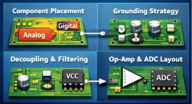
This article aims to provide a practical, engineering-oriented guide to analog PCB design, covering the process from fundamental design awareness and layout planning to specific component placement and routing strategies. Rather than focusing on theory alone, the goal is to help designers translate sound analog concepts into robust, manufacturable PCB layouts that perform reliably in real applications.
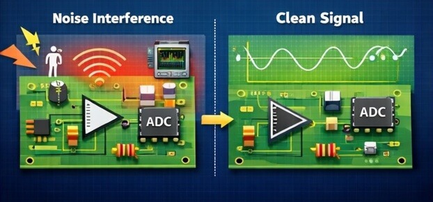
In analog circuits, there are real-world factors like voltage, current, and electromagnetic interference (EMI) that affect signal integrity. These signals generally operate at low levels, making them highly susceptible to external disturbances. For example, power supplies or inductors can emit electromagnetic fields, which may interfere with the analog signals.
Since analog signals do not operate within fixed thresholds like digital signals, they are inherently more vulnerable to noise. Any added noise or electromagnetic interference can directly degrade the circuit’s performance, affecting the desired output.
For this reason, layout, grounding, and component placement play a much more important role in analog PCB design than in digital boards.
There is a key rule during the pre-routing stage that every designer should know:
In any analog circuit, layout should be considered an integral part of the circuit.
Before starting any task, planning is essential. Similarly, when designing an analog PCB, it’s a good practice to divide the circuit into logical blocks. Below are some of the key functional blocks that should be considered:
- Power supply
- Analog input stage
- Amplifiers/filters
- Voltage or current references
- ADC / Output stage
Each block should be treated as a separate entity during placement. By following this approach, you can avoid random placement, which helps isolate sensitive sections from noise.
Additionally, it’s important to identify critical signals early in the design process. To do this, mark the following nets in your schematic:
- High-impedance inputs
- Low-level analog signals
- Voltage references
- Feedback loops
These signals require special attention during placement and routing. Identifying them in advance can help you avoid mistakes later in the design process.
Component placement may seem straightforward, but it should be done carefully, as it forms the foundation of an effective layout. Follow these guidelines when placing components to minimize noise, a major issue in analog design. Always place components according to the signal flow order, which is as follows:
Input → Conditioning → Amplification → Output
By following this practice, trace lengths will be minimized, and unnecessary crossings will be reduced.
Sensitive components, such as the op-amp and its feedback resistors, or the ADC and its reference capacitor, should be placed close to each other. Keeping the distance short helps reduce parasitic capacitance or inductance, thereby improving signal stability and accuracy.
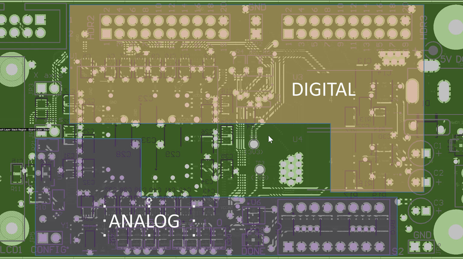
Noisy and quiet components should be kept isolated from each other. For example, switching regulators, oscillators, and digital ICs generate noise. These components should be placed away from analog inputs or near the board edges, ensuring clear separation from sensitive analog sections. Placing a switching regulator directly under or next to an op-amp or ADC input is not recommended.
One of the most common and effective practices in analog PCB design is using a solid ground plane. It provides a low-impedance return path, reduces loop area, and minimizes noise coupling. Whenever possible, dedicate one full PCB layer to ground, creating a continuous reference plane for all components.
Splitting ground planes often causes more problems than it solves. When a signal crosses a split in the ground plane, its return current is forced to find an alternative path. This increases loop area and can introduce noise and instability into the circuit. For this reason, a single, solid analog ground plane is generally recommended.
In mixed-signal designs, digital ground should be connected to the analog ground at a single, controlled point. This approach helps prevent digital switching noise from coupling into sensitive analog sections.
Decoupling capacitors should be:
- Placed as close as possible to the IC power pin
- Connected using short, wide traces
- Referenced directly to the ground plane
A common mistake is placing capacitors physically “near” the IC while routing long traces to them. The purpose of placing a decoupling capacitor close to the IC is to maintain a short current path. Long routing distances increase parasitic inductance, which significantly reduces the effectiveness of the capacitor and defeats its purpose.
A common best practice is to use multiple capacitor values on each power rail:
- A 0.1 µF ceramic capacitor at each IC power pin
- A 1–10 µF bulk capacitor per power rail section
This combination helps filter both high-frequency and low-frequency noise.
When analog and digital circuits share the same power supply, it is good practice to insert a ferrite bead or a small series resistor between the rails, followed by local bulk and ceramic capacitors. This approach helps prevent digital switching noise from contaminating the analog supply.
Analog signal traces should be kept short and direct to reduce noise pickup, minimize parasitic effects, and improve signal integrity. Avoid unnecessary detours, loops, or decorative routing.
Right-angle corners should generally be avoided. Instead, use 45-degree bends or curved traces. While right angles are not always catastrophic, smoother routing helps reduce impedance changes and improves manufacturability.
Maintaining adequate spacing between signals helps prevent many issues. Sensitive analog traces should be routed away from clock lines, high-speed digital signals, and switching power traces.
If a crossing is unavoidable, route the signals at right angles and on different layers to minimize coupling.
High-impedance nodes are extremely sensitive to leakage and noise. Best practices for these nodes include:
- Keeping traces very short
- Avoiding vias whenever possible
- Using guard rings connected to ground around critical nodes
- Keeping the solder mask clean and intact
Note: Even small amounts of contamination or moisture can significantly affect high-impedance signals.
The feedback loop area should be kept as small as possible because the feedback path largely determines amplifier stability. To achieve this, follow these guidelines:
- Feedback resistors should be placed close to the op-amp pins.
- The loop path should be kept as small as possible.
- Avoid placing vias inside the loop.
Even if multiple op-amps share the same supply, each op-amp should have its own local decoupling capacitor near its supply pins.
Place reference components early in the layout process because the voltage reference largely determines system accuracy. As a best practice, place the reference IC close to the ADC, and put decoupling capacitors immediately next to the reference pins.
Keep ADC inputs as clean and noise-free as possible. To achieve this, place anti-aliasing filters close to the ADC inputs, keep source impedance within datasheet limits, and avoid routing digital signals near ADC pins.
Another factor to consider in analog design is the thermal and mechanical effects of components. As temperature changes, analog performance can drift. Design considerations include:
- Keep heat-generating components away from precision analog parts.
- Avoid connecting large copper pours directly to sensitive resistors.
- Use symmetrical layouts for matched components.
Some common beginner mistakes include:
- Treating analog layout the same as digital layout
- Placing components randomly and routing later
- Ignoring return current paths
- Overusing ground splits
- Skipping test points during design
Avoiding these mistakes will dramatically improve the first-time success of your analog PCB design.
Analog designers should not view PCB design as mysterious—but it is unforgiving. Successful analog PCB designs come from careful planning, disciplined placement, clean grounding, and thoughtful routing. If you follow the guidelines outlined in this article, you can build analog PCBs that are stable, accurate, and reliable.
Remember: good analog performance is built into the layout, not fixed later.
If you need professional support, PCBCool offers PCB manufacturing and assembly services tailored for analog systems, with a focus on low-noise layouts, precision reference routing, and robust grounding strategies.
Reach out to PCBCool to turn your analog design into a production-ready PCB.