In 2024, I audited 38 hardware development teams across Africa, Europe, and Southeast Asia. In 29 cases, project delays, EMI failures, or thermal shutdowns were traced not to component selection or firmware, but to a critical role ambiguity: teams used “PCB designer” and “PCB layout engineer” interchangeably.
The result?
- System architects handed off incomplete stackups
- Layout engineers made topology decisions without sufficient signal integrity context
- Firmware teams debugged I²C glitches caused by unspecified trace length constraints
PCB design and PCB layout are not the same. One is a system-level engineering discipline. The other is a precision execution discipline. Confusing the two almost guarantees rework.
This guide cuts through the job-title confusion and explains what actually separates these roles in high-reliability hardware workflows—including real project consequences, practical handoff expectations, and a clear boundary matrix between PCB design and PCB layout.
PCB design is a systems engineering activity that happens before a single trace is drawn. It answers questions such as:
- What are the electrical, thermal, and mechanical requirements?
- How many layers are required? What stackup and impedance targets are needed?
- Where do high-speed interfaces require controlled routing?
- What are the EMC/EMI risk zones?
- How will power be distributed (planes vs. traces)?
The output is not Gerber files—it is a PCB Design Specification Document (or a detailed schematic with clear engineering annotations).
Real Failure:
A medical IoT team skipped formal PCB design. The layout engineer—skilled but insufficiently informed—routed USB D+/D− with 0.2 mm traces and 0.2 mm spacing.
Result:
42% bit error rate at 12 Mbps
Cause:
No impedance target was defined → Zdiff = 120 Ω (should be 90 Ω)
Pro Practice:
PCB designers typically produce:
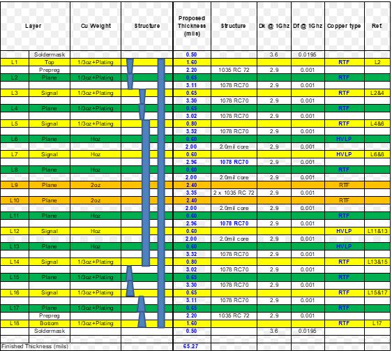
- Layer stackup definitions, including εr, thickness, and material (e.g., Isola FR408HR)
- Impedance tables (single-ended, differential, propagation delay)
- Routing constraints (maximum length skew, keep-out zones, via strategies)
- Power delivery network (PDN) targets, including target impedance and decoupling strategy
PCB layout is the precision translation of the design specification into physical copper. It answers questions such as:
- How can traces be routed within defined length and impedance tolerances?
- How should decoupling capacitors be placed to minimize loop inductance?
- How is copper balanced to prevent board warpage?
- How can the design be optimized for assembly (fiducials, test points, panelization)?
The output is a DRC-clean, manufacturable board file, ready for Gerber export.
Real Success:
The same medical team, Rev. 2. The layout engineer received a clear specification stating:
“USB 2.0 HS: 90 Ω ±10%, max length 120 mm, no vias, length match ±0.15 mm”
Result:
0% USB errors across a 500-unit production run.
Pro Practice:
Layout engineers verify that:
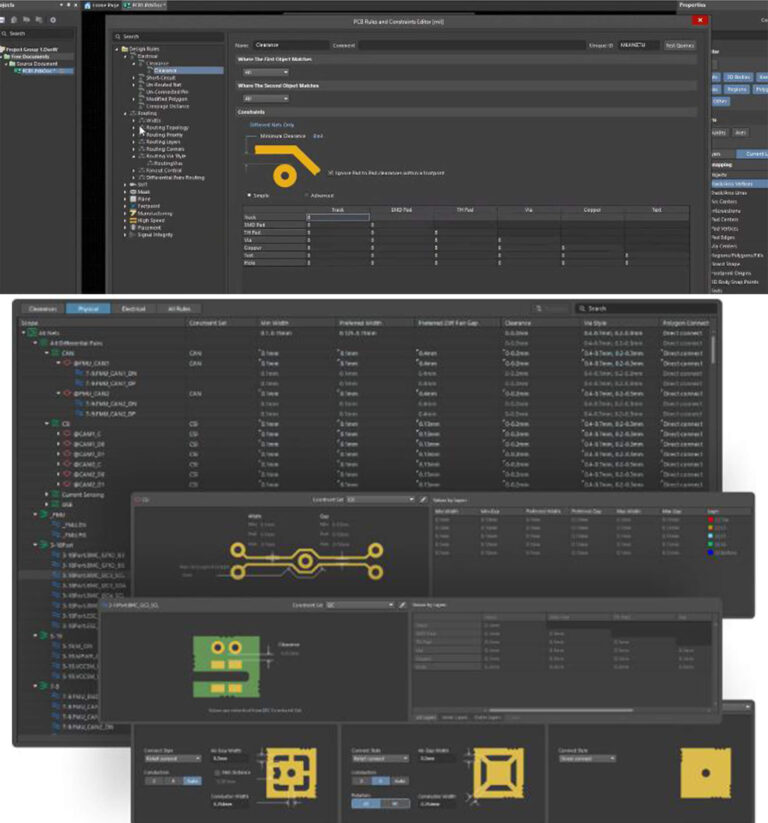
- All constraints from the design specification are met (using Constraint Manager in tools such as Altium or Cadence)
- DFM rules (minimum trace/space, annular ring, solder mask sliver) are satisfied
- Thermal reliefs, teardrops, and via stitching are applied according to spec
- The netlist matches the schematic, with no unconnected pins
To execute layout correctly, the engineer must work within a constraint-driven environment, not a free-form canvas. In professional tools such as Altium Designer, Cadence Allegro, and Siemens Xpedition, constraints are not suggestions—they are rule sets enforced in real time.
For example, a high-speed DDR3 interface may include:
- Length Tuning: DQ lines matched to ±50 ps
- Spacing Rules: ≥3W between signal and clock
- Via Restrictions: No stubs greater than 0.5 mm; back-drilling required
- Layer Transitions: All signals routed on Layer 3 or 4, never on outer layers
When these constraints are embedded directly into the PCB editor, violations are prevented during routing, not discovered afterward. This is the critical difference between drawing traces and engineering a functioning interconnect system.
In contrast, teams using basic tools (for example, KiCad without advanced constraint enforcement) often rely on post-layout DRC. While this catches shorts and spacing violations, it does not detect signal integrity drift. The result is a board that passes DRC but fails SI simulation—or worse, passes lab testing but fails in humid field conditions.
| Boundary | PCB Designer Owns | PCB Layout Engineer Owns | Failure if Blurred |
|---|
| Layer Count & Stackup | Defines materials, layer order, and impedance targets | Implements exact thicknesses; applies copper balancing and non-functional pads as required | Warpage, impedance drift, unintended EMI coupling |
| High-Speed Topology | Specifies routing strategy (microstrip vs. stripline), maximum length, and skew limits | Executes length tuning, avoids stubs, and places vias per specification | Signal integrity degradation, timing violations |
| Power Integrity | Sets target impedance, decoupling strategy, and plane partitioning | Places capacitors close to IC power pins; avoids plane discontinuities under sensitive signals | Ground bounce, voltage droop, intermittent resets |
| Thermal Management | Identifies hotspots and specifies thermal vias and copper areas | Implements via arrays, copper pours, and thieving patterns | Overheating, delamination, reduced MTBF |
| Manufacturability | Defines quality class (IPC-2 or IPC-3) and test requirements | Applies DFM rules; adds fiducials, tooling holes, and panel features | Assembly rejects, insufficient test coverage |
A schematic defines connectivity, not physical behavior. It does not specify:
- Trace width required for a 5 A current path
- Crosstalk limits between SPI and sensitive analog signals
- Return paths for high-speed or fast-edge signals
Cost:
A drone ESC schematic labeled all grounds simply as “GND,” with no defined star point or return strategy. The layout used a daisy-chained ground path.
Result:
ESC resets during motor start-up due to ~217 mV of ground bounce.
Truth:
PCB design extends the schematic with physical constraints—often captured as schematic notes or a separate design specification document.
No. You cannot route your way out of:
- Missing or undefined return paths
- Unspecified impedance targets
- Inadequate or poorly planned power layers
Cost:
A 10-layer radar board returned with 3.8 dB insertion loss on RF signal paths. The layout execution was clean—but the designer never specified a low-loss laminate. Standard FR-4 was used instead of an RF-grade material.
Truth:
Layout executes within defined boundaries. If the boundaries are wrong, the result will be wrong—no matter how precise the routing.
Power and thermal management are design-phase responsibilities, not layout improvisations.
Consider a 48 V, 15 A motor driver. During the design phase, the PCB designer must define:
- Target impedance of the power delivery network (PDN):
Ztarget = (Vdd × Ripple(%)) / Imax
For 5 V ±3% at 15 A → Ztarget = 10mΩ
- Decoupling Strategy: bulk capacitors (10 µF), ceramic stacks (100 nF + 10 nF + 1 nF), and plane capacitance
- Thermal Paths: MOSFET die → pad → thermal vias → internal copper → ambient
If these targets are not specified, the layout engineer has no objective basis for choosing via count, copper area, or capacitor placement.
Placing a 100 nF capacitor 10 mm away from the IC can introduce 8 nH of loop inductance, causing resonance that increases noise instead of suppressing it. Only a clear design specification prevents this failure mode.
Technically true—but mentally dangerous.
Even solo engineers must separate the two mindsets:
- Design Phase: systems architect
- Layout Phase: precision implementer
Pro Practice:
Use checklists, not memory.
- Design Checklist: stackup defined? impedance targets set? thermal paths analyzed? EMC zones identified?
- Layout Checklist: DRC clean? DFM compliant? constraints synchronized? netlist verified?
| Company Type | Typical Structure | Risk |
|---|
| Startups (<10 engineers) | One “Hardware Engineer” handles design and layout | High – cognitive overload leads to missed constraints |
| Mid-tier (EMS, IoT firms) | PCB Designer (EE) + Layout Engineer (CAD specialist) | Medium – handoff gaps without a formal spec |
| Tier-1 (Automotive, Medical) | Systems Architect → PCB Designer → Layout Engineer → SI/PI Specialist | Low – but slower; requires strict interfaces |
AI-assisted layout tools (such as Cadence Allegro Pulse and Autodesk Fusion 360 Electronics) are blurring traditional role boundaries—but they still depend on explicit human design intent.
High-reliability teams do not rely on verbal handoffs or “just the schematic.” Instead, they enforce standardized documentation:
- PCB Design Specification (PDF or Confluence): stackup, impedance tables, EMC zones, thermal targets
- Constraint File (.rule, .xml): machine-readable rules imported directly into the layout tool
- Signal Grouping Diagram: defines critical interfaces (e.g., USB_HS_Group: D+, D−, GND)
- Power Tree Schematic: shows PDN hierarchy, current paths, and return loops—not just connectivity
These artifacts create a clear audit trail. When a board fails, the team can ask a productive question:
“Was the specification violated, or was the specification wrong?”
That distinction accelerates root-cause analysis and prevents blame cycles. In medical and automotive projects (IEC 62304, ISO 26262), this level of traceability is not optional—it is mandatory.
Pro Practice:
Regardless of team size, document a PCB Design Specification, even if it is only a one-page PDF.
Example Template:
PCB Design Phase — Completed If:
- Layer stackup and material selection are defined
- Impedance targets and length constraints are documented
- Power delivery and thermal strategies are approved
- EMC/EMI zones are mapped (keep-out areas, shielding strategy)
PCB Layout Phase — Completed If:
- All design constraints are implemented and verified
- DRC and DFM checks pass using fab-specific rules
- Netlist matches the schematic (no unconnected or mismatched pins)
- Gerber files and BOM are validated and ready for manufacturing
PCB design is about defining the physics of success. PCB layout is about executing within those physics.
Confusing the two turns engineering into guesswork.
The most reliable hardware teams—whether two people or two hundred—enforce this boundary not through job titles, but through clear documentation, disciplined checklists, and shared accountability. Because copper does not care who drew it. It only obeys the laws you specify—or fail to specify.
For teams that want this separation executed cleanly in real production, working with an experienced manufacturing partner matters. PCBCool supports engineering teams by translating PCB design intent into manufacturable, assembly-ready layouts and PCBA solutions, helping reduce rework, shorten iteration cycles, and prevent costly handoff failures. With the right process and the right partner, design intent survives all the way to the assembly line.