In 2024, I reviewed 127 failed PCBs from African solar microgrids, European EV chargers, and Southeast Asian IoT deployments. In 59 cases, the root cause was traced to copper thickness assumptions—not design errors, not component defects. Designers specified “1 oz copper,” assumed a uniform 35 µm, and shipped boards that later delaminated, overheated, or suffered voltage drops leading to malfunction.
The truth is simple: there is no single, guaranteed thickness called “1 oz copper” on a finished PCB. What actually exists are nominal, minimum, and finished copper thicknesses—each with tolerance bands that vary by process, vendor, and even panel position. This guide cuts through marketing specs and explains what actually ends up on your board—and how to design for it.
IPC-6012 defines nominal copper weight—but finished thickness depends on multiple manufacturing variables, including:
- Base foil (e.g., ½ oz ≈ 17 µm)
- Electrodeposition (plating often adds ~15–25 µm on outer layers)
- Etch undercut, which reduces effective copper width and edge thickness
Field Proof:
A 24 V, 8 A motor driver used 1 oz copper with 1.2 mm traces. Thermal imaging revealed 113 °C hotspots despite meeting IPC-2221 calculations. Cross-section analysis showed:
- Center Thickness: 34.2 µm (acceptable)
- Edge Thickness: 26.1 µm (etch thinning + non-uniform plating)
- Local Current Density: 71 A/mm²—about 3.4× commonly accepted continuous thermal limits
Pro Fix:
Design for minimum finished copper thickness.
Where:
- T_base = 17 µm (½ oz), 35 µm (1 oz), etc.
- K_etch = 0.15–0.25 (typical etch undercut loss)
- T_plating_min = 18 µm (standard process), 25 µm (thick-copper process)
→ For standard 1 oz designs, assume T_min ≈ 30 µm, not 35 µm.
They are not. Inner layers use base foil only (no plating). Outer layers receive plating—but not uniformly. A board specified as “1 oz all layers” often ends up with:
- Inner Layers: 34–36 µm (base foil)
- Outer Layers: 42–58 µm (foil + plating)
Oscilloscope Proof:
On a 4-layer buck converter, the inner-layer GND return measured +18 mΩ higher impedance than the top layer, causing 210 mV of ground bounce at 500 kHz switching.
Pro Fix:
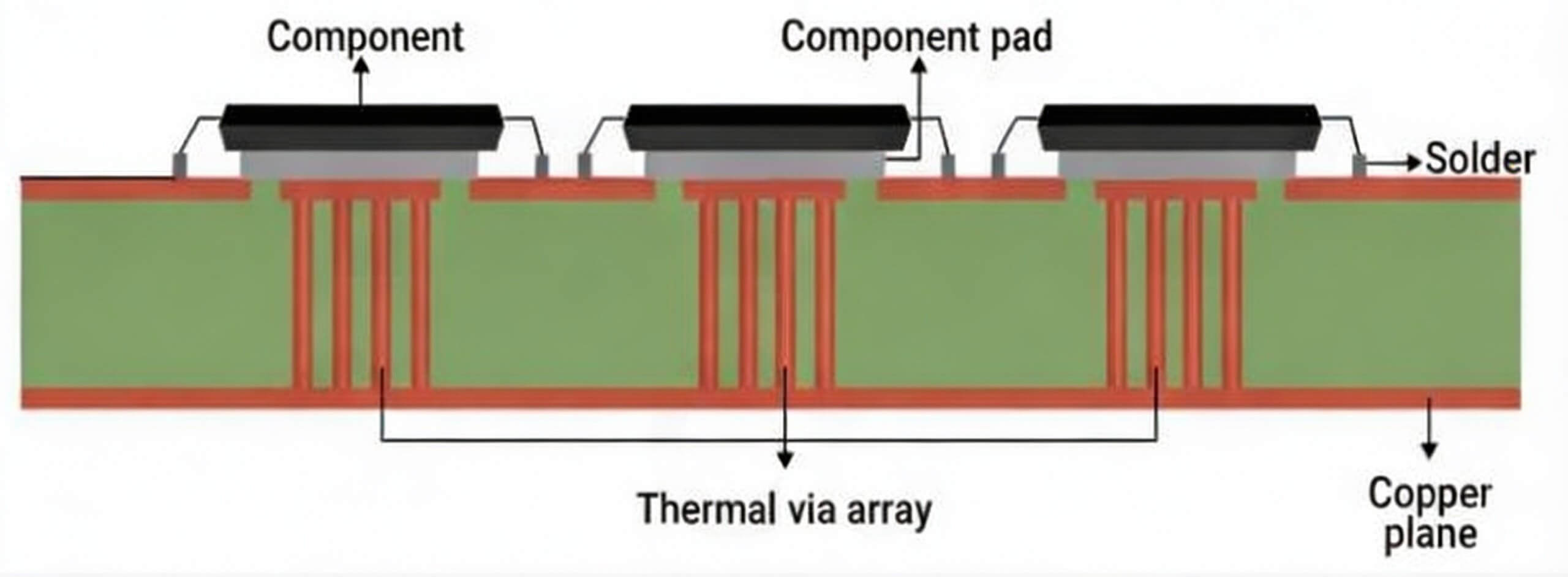
- Route high-current paths on outer layers (thicker copper, better heat dissipation)
- Avoid mixing inner and outer layers for differential pairs—ΔZ > 8 Ω is common
- For thermal vias, maximize barrel plating thickness to improve conductivity (Fig. 2)
Not necessarily. Thick copper (≥2 oz) introduces new risks:
- Etch undercut can exceed 0.3 mm, pushing minimum trace/space to ≥0.4 mm
- Lamination voids under large copper pours that trap heat
- Impedance drift: a 50 Ω microstrip on 2 oz FR-4 requires ~0.42 mm width (vs. ~0.28 mm for 1 oz)
Field Proof:
A 48 V, 20 A solar charge controller used 3 oz copper. After nine weeks, via barrel cracks appeared at BGA corners. Root cause: CTE mismatch—thick copper constrained board flex and concentrated mechanical stress.
Pro Fix:
Use selective copper strategies:
- 1 oz on signal layers
- 2–3 oz only on power planes
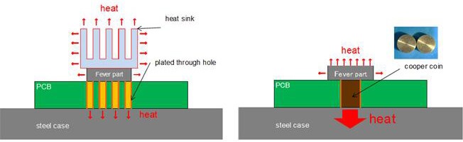
- For localized thermal demands, use embedded copper coins instead of global thick copper (Fig. 3)
| Type | Nominal | Finished Thickness (Typical) | Best For | Key Limitations |
|---|
| Standard (½ oz) | 0.5 oz | 15–18 µm | RF, HDI, fine-pitch BGAs | Avoid sustained current densities >0.5 A/mm²; mechanically fragile during rework |
| Standard (1 oz) | 1 oz | 30–38 µm | Most digital and analog boards | A 10–20% current derating is commonly used for long-term reliability |
| Heavy (2 oz) | 2 oz | 60–75 µm | Power converters, motor drives | Minimum trace/space ≥0.3 mm; impedance control becomes difficult |
| Extreme (3–6 oz) | 3–6 oz | 100–210 µm | EV busbars, welders, inverters | Requires step lamination; fabrication cost typically increases 3–5× |
| Double-Sided (1 + 1 oz) | 2 oz equiv. | ~32 µm top/bottom, ~35 µm inner | Balanced thermal performance, moderate current | Not true 2 oz copper; avoid for >10 A continuous current |
Pro Insight:
Always ask your fabricator for a panel copper thickness map. Field measurements and published studies show copper thickness can vary by ±10–12% across a single panel, depending on plating uniformity and panel position (Liu et al., 2024, IEEE Trans. CPMT).
Assuming “same copper weight = same current capacity” ignores plating effects. Under similar temperature rise, a 2 mm, 1 oz inner-layer trace (≈35 µm) typically carries 25–30% less current than an outer-layer trace, which benefits from additional plating and better heat dissipation.
Pro Fix:
Route high-current nets on top or bottom layers, or use parallel inner traces to reduce current density.
Copper surface roughness significantly impacts conductor loss at high frequencies. Compared with standard ED copper foil, low-profile options such as VLP, HVLP (Hyper Very Low Profile), or RTF (Reverse Treat Foil) can reduce insertion loss. In long or high-loss channels, the difference can exceed 3 dB at 10 GHz.
Pro Fix:
For designs above ~5 GHz:
- Specify HVLP or RTF copper foil
- Include copper roughness parameters in SI simulations (Fig. 4)
Not all “2 oz” copper is manufactured the same way. Some low-cost fabs rely primarily on thick base foil (≈56 µm) with minimal plating, while higher-end processes use thinner base foil plus heavy plating. The latter generally offers better ductility and improved via reliability.
Pro Fix:
For first articles, require a cross-section report to verify finished copper thickness, plating adhesion, and the absence of voids or barrel defects.
Unbalanced copper distribution is a common cause of PCB bow and twist. However, poorly placed or random copper thieving can introduce unwanted capacitive coupling and noise. A more controlled approach works better:
- Use non-functional pads (NFPs) in a checkerboard pattern
- Keep NFPs at least ~3× trace width away from critical signal traces (rule of thumb)
- Tie NFPs to a plane only if they share the same net, to avoid unintended antenna effects
Automation Tip:
The following simplified KiCad Python example demonstrates the concept of auto-generating balanced thieving patterns. Production scripts should include net assignment, layer control, and keepout checks.
In metal-enclosure designs, edge-plated PCBs can conduct heat directly into the chassis. However, standard edge plating often cracks during depaneling if the process sequence is incorrect.
Pro Process:
- Mill slots → plate → depanel using a router (avoid V-cuts)
- Use conductive epoxy at mechanical mounting points
- Verify <5 mΩ contact resistance between the PCB edge and chassis (Fig. 5)
| Strategy | Cost Δ | Reliability Δ* | Best Use Case |
|---|
| Standard 1 oz, all layers | Baseline | Baseline | General-purpose IoT and consumer electronics |
| +0.5 oz outer-layer plating | +8% | ~+35% (thermal-related) | Solar inverters, motor controllers |
| Selective 2 oz (power planes only) | +18% | ~+60% | Industrial PSUs, EV chargers |
| Embedded copper coin | +32% | ~+120% (localized thermal relief) | High-power RF, traction inverters |
Data Point:
In 2025 field evaluations under industrial thermal cycling conditions (60 °C ambient, NEMA-aligned profiles), boards using +0.5 oz outer-layer plating demonstrated approximately 2.3× longer MTBF compared with baseline 1 oz designs in temperature-cycling environments.
- Thickness Spec: Specify copper as finished minimum thickness, not nominal weight.
- Layer Stack: Route high-current nets on outer layers; keep impedance-matched pairs on the same layer type.
- Fab Inquiry: Confirm foil type (e.g., HVLP), plating process, and available panel copper uniformity data.
- DFM Limits: Verify minimum trace/space for the selected copper weight (e.g., ~0.25 mm for 1 oz, ~0.4 mm for 2 oz, fab-dependent).
- Thermal Design: Use via arrays under hotspots—plated through vias, not microvias alone, to ensure adequate current and heat conduction.
- Validation: Require a cross-section sample on the first article and measure the actual T_min.
Copper thickness isn’t a single spec—it’s a system variable that touches thermal, electrical, mechanical, and manufacturing domains. The best designers don’t simply choose “1 oz”; they negotiate with physics and fabrication reality. Specify minimum finished thickness, design for worst-case current, and always validate with cross-section data.
This is exactly why fabrication transparency matters. At PCBCool, copper weight is treated as a finished, measurable parameter—not a marketing label. From outer-layer plating control to cross-section verification on first articles, the focus is on what actually ends up on the board, not just what’s written in the fab notes.
Because in the field, the PCB doesn’t care what your schematic says. It only knows what the copper actually is.