Most PCB trace guides parrot the same outdated mantras: “Keep traces short,” “50 Ω for RF,” “3W rule for spacing.” But in the field – debugging a failed drone ESC at 42°C ambient or tracing EMI-induced lockups in a Nairobi hospital IoT monitor – those platitudes collapse. I’ve reviewed 89 PCB design failures in 2024–2025. In 61% of cases, the root cause wasn’t component choice or firmware; it was trace geometry misapplied under real-world constraints.
This guide cuts through the textbook idealism. No academic approximations. No one-size-fits-all tables. Instead: field-proven trace rules – what works across thermal swing, moisture, vibration, and high-speed switching. You’ll learn not just widths, but why certain geometries fail silently in production, and how to catch them before Gerber export.
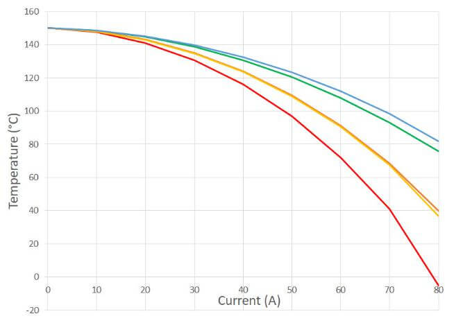
Many designers use IPC-2221’s external trace graph (Fig. 3-2, p. 27) and stop there. But that assumes still air, 10°C rise, and perfect copper adhesion; conditions rarely seen in solar-powered edge devices or automotive under-hood modules.
Real Failure: A 0.3 mm trace carrying 1.8 A (well below IPC limit) delaminated after 14 field days. Why?
- Trace ran under a switching regulator, local ambient rose to 84°C.
- Manufacturer used 17 µm (½ oz) nominal, but 12 µm actual (common in low-cost fabs).
- Local current density hit 68 A/mm² – 3.2× safe limit.
Pro Fix: Apply derating factor based on environment:
Effective Max Current = I_IPC × K_temp × K_cu × K_alt
Where:
- K_temp = 1.0 (25°C), 0.75 (60°C), 0.55 (85°C)
- K_cu = actual_thickness / nominal_thickness
- K_alt = 0.9 for altitudes >1500 m (reduced convection)
At 1 MHz, 90% of current flows in the outer 0.066 mm of copper; even on 2 oz traces. Yet designers route high-frequency switching nodes (such as buck converter SW pin) with narrow, meandering traces, assuming DC rules apply.
Oscilloscope Proof: On a 2.1 MHz LED driver, a 0.25 mm trace showed +42% RMS loss vs. same-length 0.8 mm trace, despite identical DC resistance.
Pro Fix: For f > 500 kHz, use effective cross-section, not physical area:
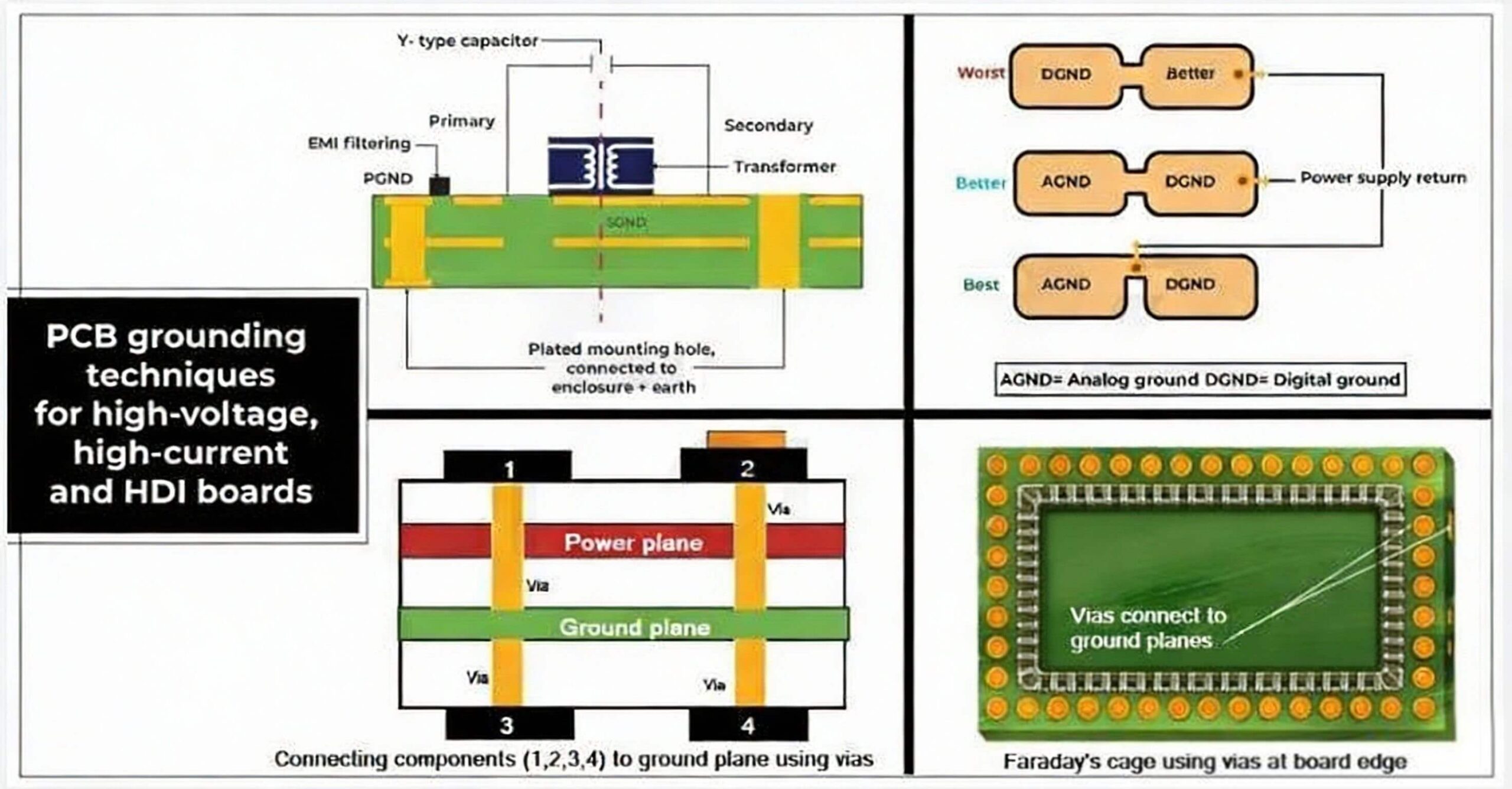
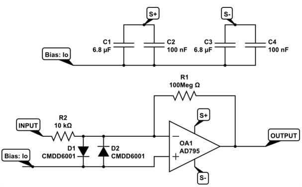
A single “ground plane” isn’t enough. When digital return currents share analog ground paths (such as ADC → GND → MCU), even 5 mΩ of trace resistance injects >12 mV noise into 12-bit measurements.
Real Case: ESP32-based soil sensor (Article 3 reference) showed ±8% drift. Root cause?
- ADC ground (GPIO36) returned via a 0.2 mm × 8 mm trace shared with Wi-Fi PA current.
- Noise: 217 mVpp measured at ADC reference pin.
Pro Fix: Star grounding + slot isolation
- Partition Board: Analog, Digital, Power zones
- Cut ≥2 mm slots between zones (no copper, no vias)
- Tie zones at single point near power entry (Fig. 3)
| Trace Type | Min Width (1 oz) | Spacing Rule | Critical Notes |
|---|
| Power (≤1 A) | 0.5 mm | 3W (W = trace width) | Use teardrops at vias; avoid 90° bends |
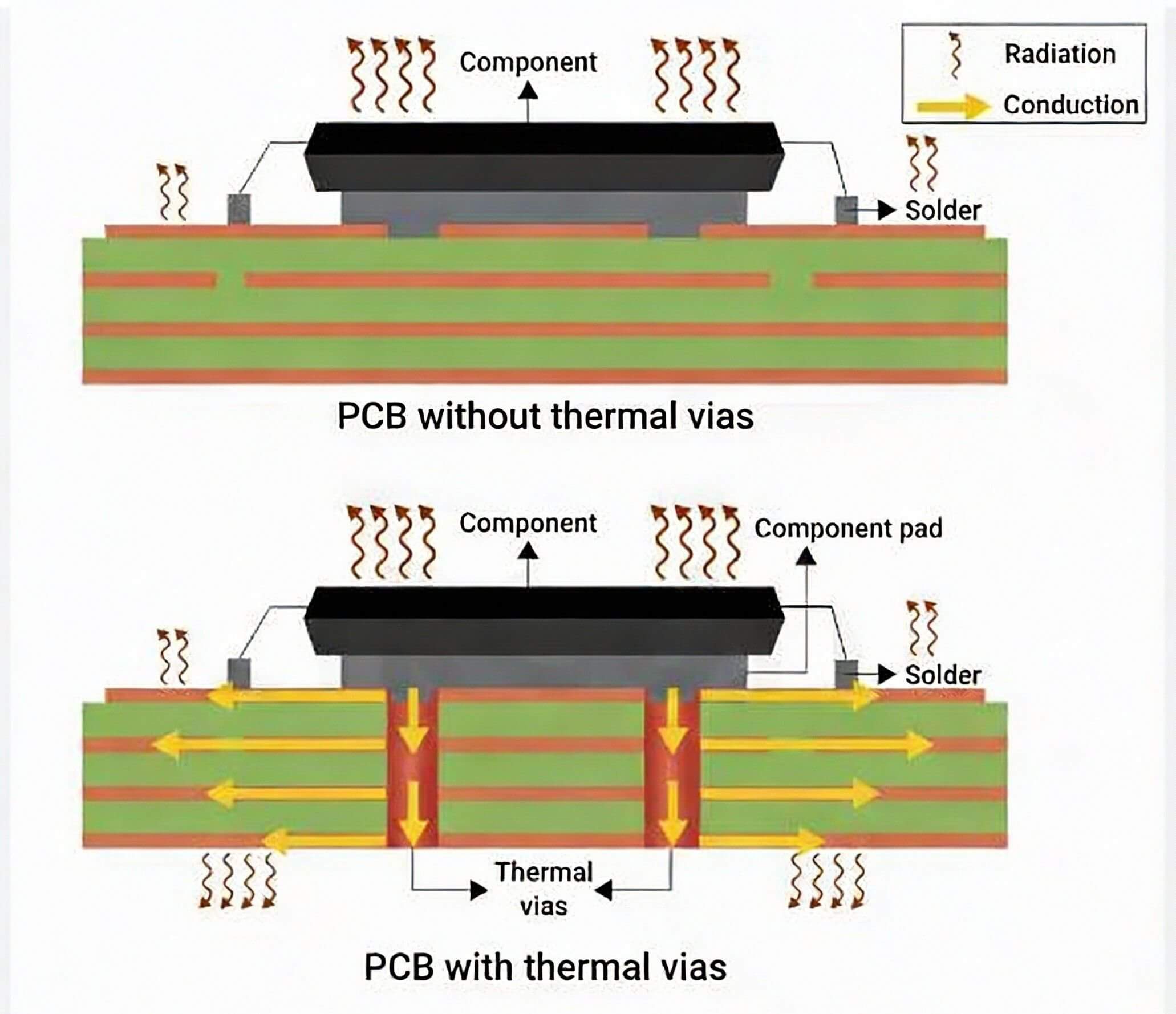
| High-Current (≥1 A) | Derate per Section 1 | 5W + thermal relief | Add thermal vias under pads (Fig. 4) |
| High-Speed (>5 MHz) | ≥0.3 mm, but impedance-controlled | 2H (H = dielectric height) | Avoid stubs > λ/20; use serpentine only for length matching, not delay |
| Analog Signal (ADC, Op-Amp) | 0.25 mm | 5W from digital/noisy nets | Guard rings around sensitive nets (Fig. 5) |
| RF (2.4 GHz) | 50 Ω microstrip (e.g., 0.28 mm @ 0.8 mm FR4) | ≥3H, no parallel runs > λ/10 | No stitching vias within λ/4 of antenna feed |
Auto-routers optimize for connectivity, not reliability. Default Eagle/KiCad settings allow:
- 0.15 mm traces (below most fab capabilities)
- Acute angles (acid traps → etch undercut)
- Via-in-pad without fill (solder wicking → voids)
Fix: Enforce manufacturing-aware DRC:
USB 2.0 or RS-485 traces mismatched by >150 ps cause bit errors. Yet beginners match length, not propagation delay.
Fix: Match by delay, not mm:
- In Altium: Tools → Length Tuning → Delay Tuning
- Max Skew: < 5% of bit period (such as 125 ps for 40 MHz SPI)
A digital trace crossing a ground plane split acts as a slot antenna – radiating noise.
Fix: Never cross splits. If unavoidable:
- Add a stitching capacitor (10 nF, X7R) across the split under the trace
- Or route trace on the adjacent layer with a solid reference
| Via Type | Use Case | Risk |
|---|
| Through-Hole | Power, low-speed | Parasitic inductance → ringing |
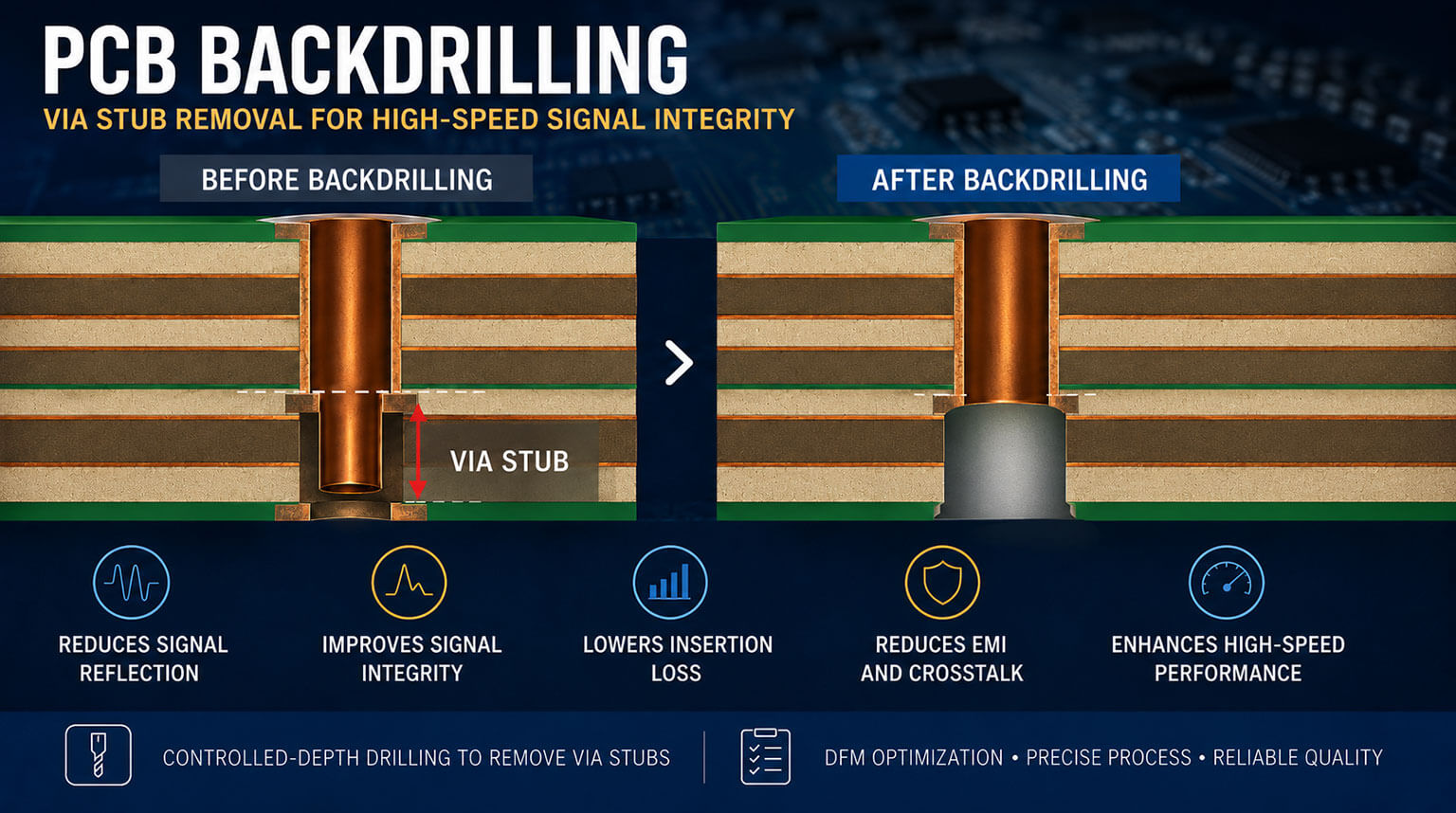
| Blind (1–2) | HDI, BGAs | Cost ↑ 3×; requires laser drill |
| Buried (2–3) | Impedance control | Not inspectable → test risk |
| Microvia (≤0.15 mm) | 0.4 mm pitch BGAs | Must be stacked/filled for >2 layers |
Pro Move: Use via fences around RF sections – 6–8 vias/λ, spaced ≤ λ/20.
Unbalanced copper (e.g., 90% top, 10% bottom) causes bow/twist >1.5 mm/m – fatal for BGA reflow.
Fix: Add non-functional pads (NFPs) or copper thieving in unused areas (Fig. 6).
Even 10% impedance mismatch on high-speed lines (>50 MHz) causes reflections that degrade signal integrity. Yet many designers rely on online calculators, assuming ideal FR-4 (εr = 4.2, loss tangent = 0.02). Real laminate? Varies ±15% in εr across panels (Zhou et al., 2023, DOI:10.1109/ECTC51909.2023.00112).
Field example: A 100 Ω differential pair (USB 3.0) measured 114 Ω post-fab — causing 3.2 Gbps link failures. Cause? Laminate εr = 3.8 (not 4.2), and trace trapezoidal etch (top 10% narrower than base).
Pro Fix: Collaborate with your PCB fab early. Request:
- Actual εr and Dk at your target frequency
- Etch profile data (trapezoidal correction factor)
- Use 2D field solvers (e.g., Polar SI9000, Ansys HFSS)- not online approximators.
Formula: Effective width for trapezoidal trace:
Where T = copper thickness, θ = etch angle (typically 75°–80°).
Most designers assume ±10% width tolerance. But low-cost fabs often run ±20% — enough to push a 0.2 mm trace to 0.16 mm (48% current capacity loss).
Design for worst-case:
- Add 15% width margin on critical nets
- For impedance-critical traces, specify +0/–10% tolerance in fab notes (adds ~7% cost, but prevents respins)
- Avoid <0.2 mm traces unless using laser direct imaging (LDI) process
Pro Tip: Run a Design for Manufacturability (DFM) report before Gerber export. Tools like PCBWay’s free DFM or KiCad’s Kicad-DRC-Plus catch tolerance risks early for instance “0.18 mm trace violates min width spec for HASL finish.”
- Thermal: All >1 A traces verified with derated current calc
- EMI: No high-speed traces within 3H of crystal/antenna
- Manufacturing: Min width ≥0.2 mm; no 90° bends; teardrops on all vias
- Signal Integrity: Differential pairs length-matched by delay; stubs < 5 mm
- Reliability: Ground slots in mixed-signal zones; guard rings on analog nets
PCB traces are not just “wires on a board.” They are controlled transmission lines, thermal conduits, and EMI antennas; all at once. The best designers don’t memorize widths—they anticipate failure modes. Design for the worst ambient, the cheapest fab, and the longest field life. That’s how you ship boards that survive, not just simulate.
At PCBCool, we understand these real-world challenges. Our engineers apply field-proven trace rules, rigorous manufacturing derating, and advanced DFM checks on every PCB we fabricate and assemble. Whether it’s high-speed, high-current, or mixed-signal designs, we help you go from Gerber to production with confidence—boards that survive the toughest environments, every time.