If you’re new to electronics or PCB design, you’ve probably asked—or will soon ask—this question: “What’s the difference between a schematic and a layout?”
At first glance, they might look similar. Both use symbols, lines, and little boxes.
But in reality, they’re completely different. Confusing the two is a classic beginner’s mistake that almost everyone makes at first.
Let’s break it down in simple terms, with clear examples you can actually relate to.
By the end of this article, you won’t just know the definitions—you’ll understand how schematics and layouts work together to bring a circuit to life.
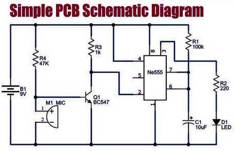
A schematic diagram is basically the blueprint for how your electronic circuit works. It’s a logical drawing, not a physical one. You won’t see actual sizes, exact locations, or physical dimensions. Instead, you see how components are connected, how signals flow, and where power and ground go.
Think of it like this: a schematic is the rough blueprint of a house. It shows which rooms are connected, where the doors go, and maybe how the wiring runs. But it doesn’t tell you the wall thickness, where the furniture is, or what materials are used.
So, what do you actually find in a schematic?
You’ll see symbols for all the components—resistors, capacitors, chips, connectors. You’ll also see lines for wires, labels like VCC or GND, and values like 10kΩ or 100nF.
Why use a schematic?
It’s how you explain how a circuit works before building anything. You can spot problems early, share your design with others, and it’s an essential step before moving on to the PCB layout. On paper, this is where everything comes together.
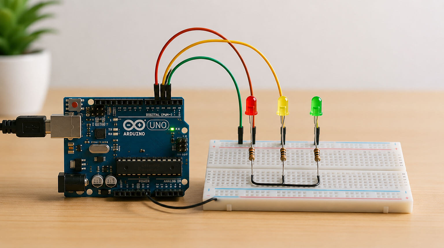
A PCB layout is where your circuit takes physical form. This is the nuts-and-bolts part—the actual design of the board itself. Here, you decide where each component goes, how the copper traces are routed, the shape and size of the board, where holes are drilled, and how many layers the board will have.

Forget the schematic for a moment—that’s just the blueprint. The PCB layout is the finished house. The walls are up, the rooms have real dimensions, and you can see exactly where the wiring runs inside those walls.
So, what does a PCB layout look like?
You’ll see realistic outlines of components, copper traces weaving around the board, pads and vias (tiny holes that let signals pass between layers), the board edges, and silkscreen markings—basically everything a manufacturer needs.
Why go through this process?
Without a carefully planned PCB layout, nothing gets built. This step ensures that all components fit, prevents shorts and electrical interference, and gets your design ready for production.
| Feature / Aspect | Schematic | PCB Layout |
|---|
| Purpose | Shows how the circuit works logically | Shows how the circuit is physically implemented |
| Representation | Symbols, lines, and component values | Realistic component outlines, copper traces, pads, vias |
| Focus | Connections, signal flow, power & ground | Component placement, routing, board shape & layers |
| Dimensions | No physical sizes or spacing | Exact sizes, spacing, and board dimensions |
| Problem Detection | Can catch logical errors or missing connections | Can catch physical issues like shorts, noise, or spacing problems |
| Analogy | Brain / blueprint | Body / finished house |
| When Used | First step in design | After schematic is complete, before manufacturing |
| Output | Diagram to explain design | Files ready for fabrication and assembly |
You can’t jump straight to the PCB layout without first having a schematic. The schematic always comes first. Here’s the typical workflow:
- Draw the schematic – figure out how all the components connect.
- Assign footprints – match each symbol in the schematic to a physical part.
- Import the schematic into your PCB software.
- Place components on the board.
- Route the connections (the copper traces).
- Check for mistakes and make sure everything works as intended.
- Generate the manufacturing files to send to your board maker.
Think of it like this: the schematic is the brain, handling the logic. The PCB layout is the body, making everything real and tangible.
When you look at both together, it all clicks. The schematic explains how the circuit works, while the PCB layout shows how everything physically fits on the finished board. That’s the key difference—and it’s what turns your idea into something you can actually hold.
This is a classic trap for beginners. You might finish your schematic and think, “Everything looks good, so the PCB should be fine, right?” Not quite. Schematics won’t tell you if your components are crowded, or if there could be noise issues, shorts, or overheating. That’s exactly what the PCB layout is for.
Even with a perfect schematic, sloppy placement on your PCB can cause problems—noise, difficult routing, overheating, or tricky assembly. You need to think about how signals flow, where the power goes, and which components should be close together. Smart placement makes the rest of the design process much easier.
Just because a symbol looks correct in your schematic doesn’t mean the physical footprint matches. Pin orders might be wrong, or the size might not fit. If you skip this step, your parts won’t fit on the board, and your design won’t work.
Many beginners dive straight into drawing traces. Don’t rush. Place all your components first, consider current paths, and then start routing. Planning before routing saves a lot of headaches later.
A schematic shows the plan—what your circuit should do.
A PCB layout shows the reality—how it actually works once built.
Think of it this way: the schematic is the idea, and the PCB layout is the reality. Both are essential—you can’t skip one or replace it with the other.
Understanding this makes PCB design much easier and even more enjoyable. And if you want to take your designs from concept to production smoothly, PCBCool can help. With professional PCB manufacturing and assembly services, we make sure your schematics turn into high-quality, ready-to-use boards without the usual headaches.