For a semiconductor company like our US client, the “Validation Gap” is the most nervous time in the R&D cycle. You have just received the first batch of prototype silicon from the foundry. These chips are incredibly expensive. They are scarce. And the engineering team is waiting to verify if the new architecture works.
To do that, you need a validation board.
The client sent us an inquiry for exactly this. The order volume was tiny—just 10 units. But the technical density was high. Each board required 300+ components, populating both the top and bottom sides.
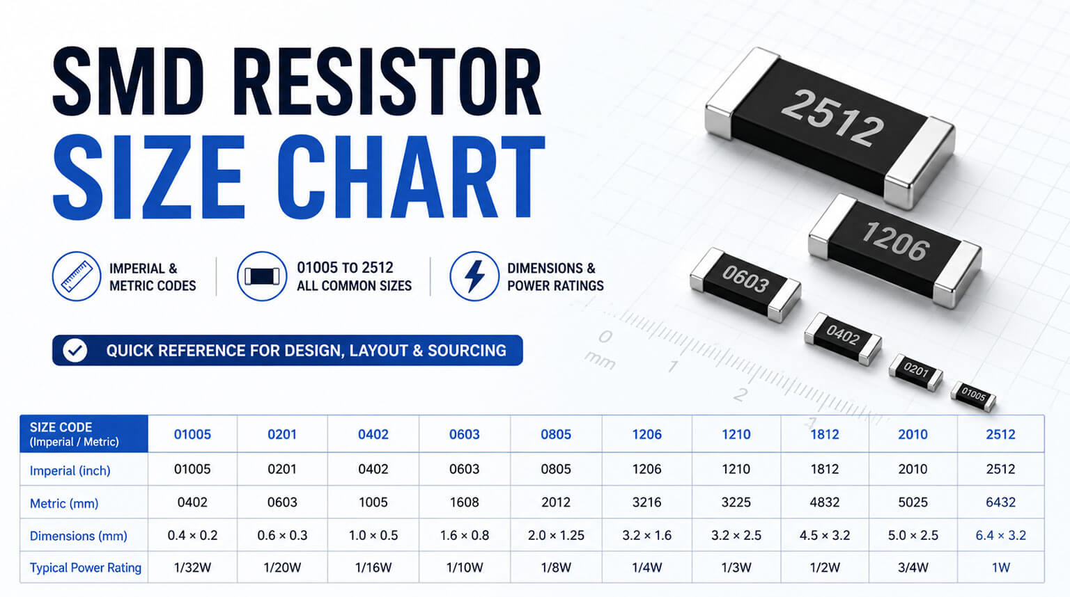
The real problem wasn’t the quantity. It was the footprint. The design featured a prototype BGA with a 0.25mm ball pitch and required extensive use of 01005 (Imperial code) passive components.
This puts the project in a difficult spot.
- Standard Prototype Shops: They can deliver fast (24-48 hours), but their process capability usually stops at 0.4mm pitch. They rarely have Type 6 paste or X-ray inspection.
- Tier 1 EMS: They have the technology, but they aren’t interested in a 10-piece order. Even if they take it, their NPI (New Product Introduction) setup takes 3-4 weeks.
The client needed a Quick Turn PCB assembly solution that could handle Fine Pitch BGA Assembly in 7 days.
Here is the engineering breakdown of how we solved it.
When we reviewed the Gerber files, we identified three primary constraints that made this a “High-Mix Low-Volume” nightmare for standard assembly lines.
| Feature | Specification | Why it’s Hard |
|---|
| BGA Pitch | 0.25 mm | The gap between balls is so small that standard solder paste won’t release from the stencil. |
| Passives | 01005 (0.4 x 0.2 mm) | Mass is 0.04 mg. They are prone to “tombstoning” (standing up) if airflow or heat is uneven. |
| Structure | Double-Sided SMT | The board goes through the oven twice. The first side risks oxidation or parts falling off during the second pass. |
| Material | Prototype Silicon | Zero Defect requirement. We cannot simply “rework” a damaged prototype chip. |
The first hurdle was getting the solder paste onto the PCB. For a 0.25mm pitch BGA, the physics of solder paste printing starts to fail.
To get a good print, the solder paste must release from the stencil aperture and stick to the PCB pad. This is governed by the Area Ratio (AR).

Industry standard (IPC-7525) says AR must be >0.66.
Let’s look at the numbers for this project:
- Aperture Diameter: 100 µm (0.1 mm) for a 0.25mm pitch.
- Standard Stencil Thickness: 100 µm (0.1 mm or 4 mil).

Result: 0.25 is way below 0.66.
If we used a standard process, the solder paste would clog the stencil. The BGA pads would get little to no solder, resulting in Non-Wet Open (NWO) defects.
We couldn’t change the BGA pitch, so we had to change the materials.
Most assemblers use Type 4 solder paste (particle size 20–38 µm). It’s cheap and stable. But for this build, Type 4 particles are too big for the 100 µm holes.
We switched to Type 6 Lead-Free Solder Paste (SAC305 alloy).
- Particle Size: 5–15 µm.
- Benefit: The “dust-like” consistency allows it to pack into the tiny apertures and release cleanly.
(Note: Type 6 paste is expensive and sensitive. It has a shorter shelf life and reacts faster to oxidation. We have to keep it refrigerated at 4°C and only remove it right before the print cycle.)
We also modified the stencil fabrication method. A standard laser-cut stencil has rough walls (micro-burrs) that hold onto the paste.
We utilized a SUS301 Stainless Steel stencil with Electropolishing. The electropolishing process smooths the aperture walls, reducing surface tension friction and allowing the paste to slide out.
The second major risk was the 01005 capacitors. These parts weigh 0.04 mg. The surface tension of molten solder is strong enough to lift them vertically—a defect called “tombstoning.”
Why it happens
Tombstoning is a timing problem. If the solder on the left pad melts 0.5 seconds before the solder on the right pad, the wetting force pulls the component up.
This usually happens due to bad PCB Layout: if one pad connects to a thin trace and the other connects to a large copper ground plane, the ground plane acts as a heatsink, delaying the melt.
Before we cut the stencil, our DFM (Design for Manufacturability) engineers reviewed the Gerber files. We found 3 areas where the pad definitions for the 01005s were risky.
- Issue: Asymmetrical thermal relief.
- Action: We flagged this to the client . We recommended modifying the mask openings to ensure “Absolute Bilateral Symmetry”.
- Rule of Thumb: For 01005s, the solder mask opening should be Non-Solder Mask Defined (NSMD) or strictly controlled to ensure equal copper exposure.
Putting these parts on the board requires extreme delicacy.
- Force Control: We set the Pick-and-Place nozzle force to 1 Newton. Standard force (3-4N) would crack the ceramic body of an 01005.
- Vision System: Standard vacuum checks don’t work well here—the part is too small to block the airflow reliably. We used Laser Alignment to verify the part was on the nozzle before placement.
Soldering in air is fine for big resistors. For 0.25mm BGAs and 01005s, it is a recipe for failure. The oxygen causes rapid oxidation on the tiny solder powder spheres of the Type 6 paste.
We used a Nitrogen (N2) Reflow process. But you can’t just blast pure nitrogen.
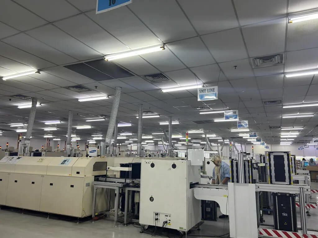
There is a specific window for Oxygen concentration: 1,000 to 2,000 ppm.
- Scenario A: Too Clean (< 500 ppm O2)
If the environment is too pure, the wetting tension becomes too strong. The solder snaps to the pad instantly. This aggressive wetting actually increases the torque on the 01005s, causing more tombstoning.
- Scenario B: Too Dirty (> 3000 ppm O2)
The Type 6 paste powder oxidizes. This leads to “Graping” (where the solder looks like a bunch of un-melted grapes) and Head-on-Pillow defects on the BGA.
We set our ovens to maintain a steady 1500 ppm O2. This gave us the “Goldilocks” zone: good wetting for the BGA, but manageable surface tension for the 01005s.
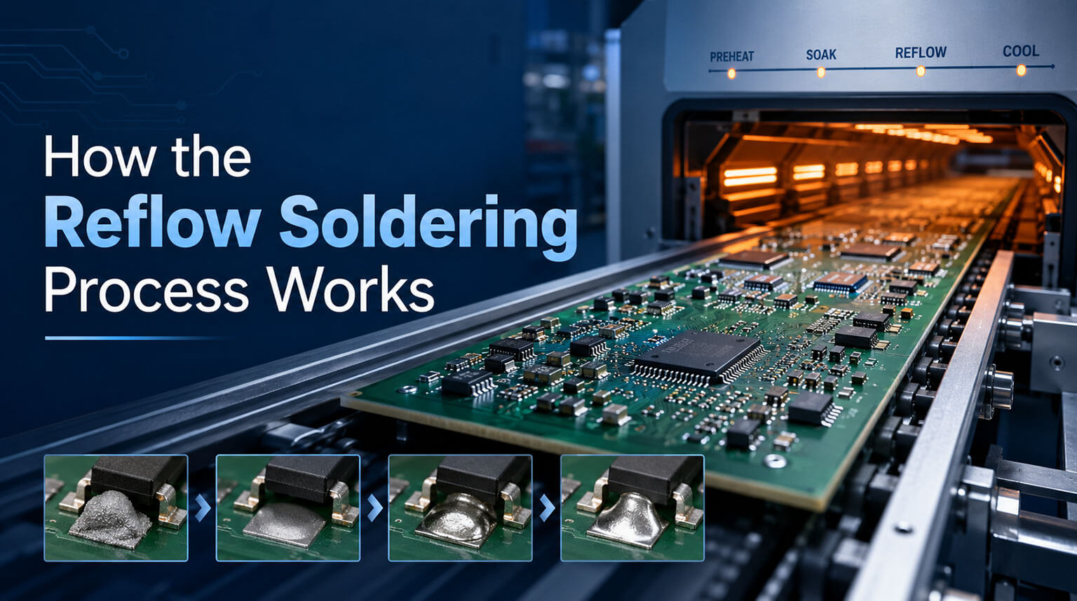
We also used a “Soak” profile instead of a linear ramp. We held the temperature between 150°C and 200°C for 90 seconds.
This pause allows the PCB copper, the BGA body, and the tiny passives to all reach the same temperature before the solder melts. Thermal equilibrium is the best defense against tombstoning.
For a Semiconductor Validation Board Assembly, you cannot assume a joint is good just because it looks okay. The critical joints are hidden under the BGA.
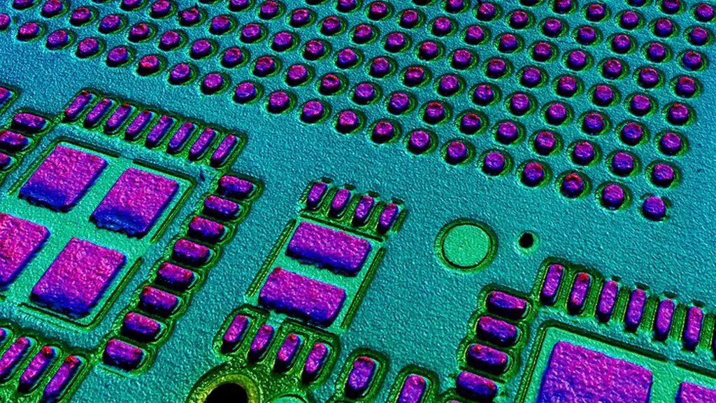
We inspected the solder paste deposition before placing components.
- Why: If the print is bad, wiping the board and re-printing costs $5. If we find the defect after reflow, the board is scrapped (costing thousands).
- Standard: We looked for volume consistency. Any pad with <70% volume was rejected.
100% AXI (Automated X-ray Inspection)
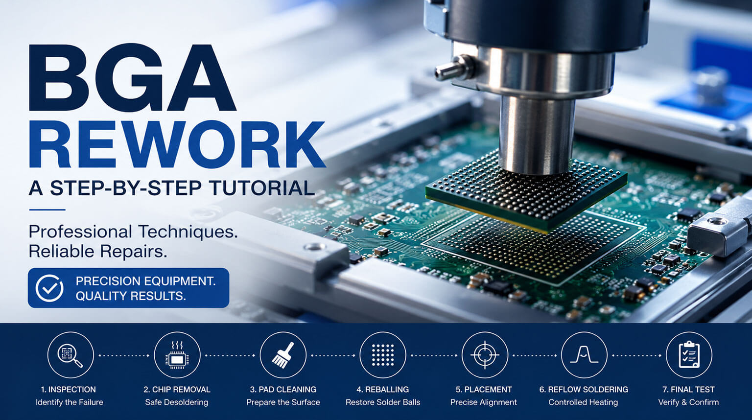
This was mandatory. We X-rayed every single BGA.
We were looking for two specific killers:
- Head-on-Pillow (HoP): Where the BGA ball rests on the solder paste but doesn’t fuse. It creates an intermittent electrical connection that drives validation engineers crazy.
- Voiding: Air bubbles trapped in the joint. We verified that total voiding was ≤ 15% of the joint area.
The project moved through our Turnkey NPI Manufacturing line quickly.
- Day 1-3: PCB Fabrication (Quick turn, ensuring planar VIP pads). Sourcing components from Digi-Key/Mouser.
- Day 4: DFM Review & Stencil Fabrication (Electropolished).
- Day 5: SMT Assembly (Top Side).
- Day 6: SMT Assembly (Bottom Side) & X-Ray Inspection.
- Day 7: Final FCT (Functional Test) & Shipping.
We delivered all 10 boards on time. First Pass Yield was 100%.
For the client, this meant they could start silicon validation immediately, without wondering if a board assembly error was masking a chip bug.
If you are designing validation boards with 0.3mm pitch or smaller, don’t leave the assembly to chance. Contact PCBCool for a free DFM review of your next NPI build. We can spot the risks before you cut the stencil.