TM had a problem.
They needed to build the “Hammerhead Dyno,” a piece of precision audio measurement equipment. The specs were tough, the volume was low, and the physics were fighting against the manufacturing process.
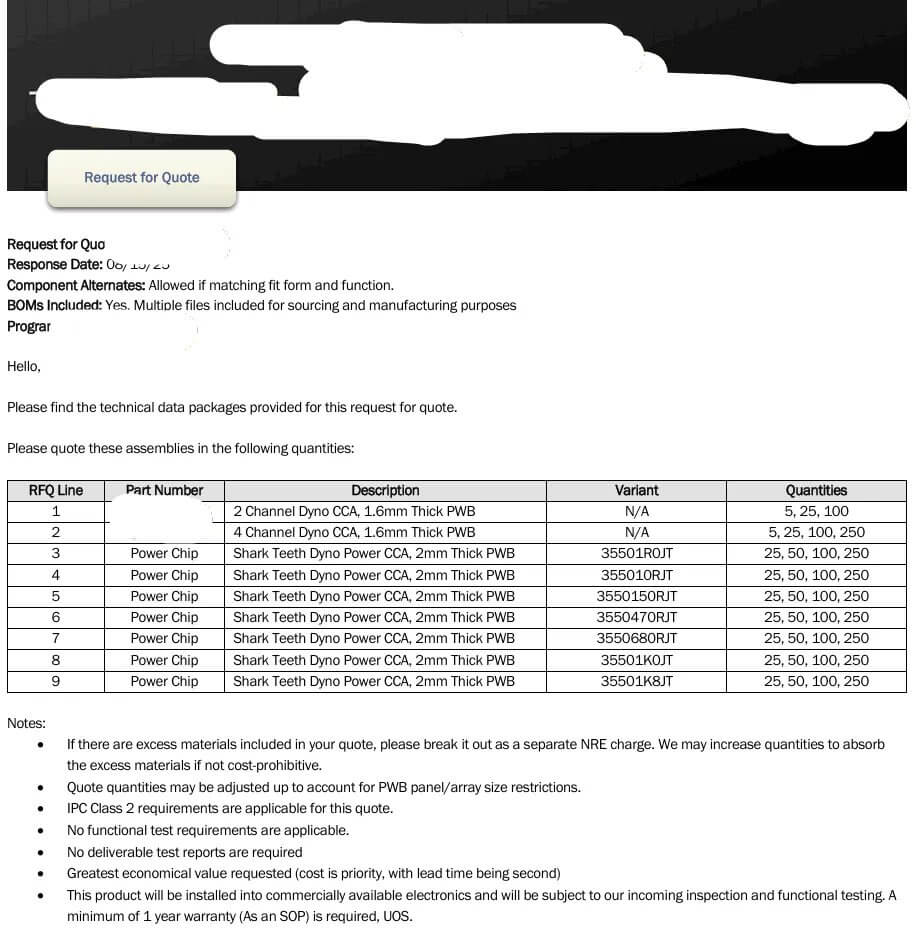
This wasn’t a standard “print and place” job. The design called for Low Volume PCB Assembly (batches of 25 to 100 units) but demanded the reliability of industrial power electronics. The board was 2.0mm thick—significantly thicker than the standard 1.6mm—and populated with massive TE Connectivity 3550 series power resistors.
We didn’t just accept the Gerber files and run the machines. That would have failed. We had to re-engineer the assembly process, specifically regarding Heterogeneous Panelization and High-Thermal-Mass Assembly, to make the economics work and keep the physics in check.
Here is the breakdown of how we handled the engineering trade-offs, the failures we avoided, and the data behind the decisions.
The first issue wasn’t technical; it was financial. TM’s RFQ listed seven different resistance variants (1.0Ω, 1.8Ω, 4.7Ω, etc.) for the same form factor.
In a standard PCBA factory workflow, every unique SKU is treated as a separate job.
The Math:
- Laser Stencil: ~$80 – $150 per design.
- Machine Setup (Pick & Place + Reflow): ~$100 – $200 per run.
- Total NRE (Non-Recurring Engineering) per variant: ~$250.
- Total for 7 variants: $1,750 just to turn the machines on.
For a startup running 25 units of each, that NRE cost adds nearly $10 per board before you even pay for the components or the bare PCB. That kills the margin.
We couldn’t treat these as seven jobs.
The technical problem was harder. Audio PCBA Manufacturing requires signal integrity, and for a dummy load (a device that absorbs power to test amplifiers), that means thermal stability.

The design used a 2.0mm FR-4 substrate. This adds rigidity, which is good. But thermally, it acts like a heat sink during the soldering process. It sucks the heat out of the solder paste before it can wet to the pad.
Then there are the TE 3550 resistors. These are Bottom Terminated Components (BTCs) with large thermal pads. The connection between the component and the board is the main path for heat to escape.
If that solder joint has bubbles (voids), the heat can’t get out.
- The specific risk: Flux gas gets trapped under the large pad during reflow. Gas has terrible thermal conductivity compared to solder alloy.
- The consequence: A void creates a “heat flux bottleneck.” Current gets forced through a smaller area, creating hotspots. If the void area exceeds 20-50%, the die temperature spikes.
- The Audio Impact: As the resistor heats up, its resistance changes (Temperature Coefficient of Resistance, or TCR). If the resistance drifts, the Dyno gives false readings.
TM stated: “No Functional Test required.” (This is always scary for a manufacturer. It means if we make a mistake, we won’t catch it until the customer plugs it in. We had to be sure.)
Standard approach: build each variant on separate panels, pay seven NRE fees.
Our approach: combine all seven designs onto one “family panel” using heterogeneous panelization.
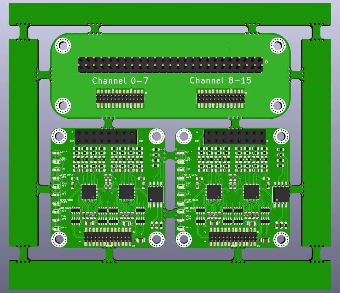
Panel Layout Comparison
| Approach | Units per Panel | Material Waste |
|---|
| Single variant (7 panels) | 45 each | 12% |
| Family panel (combined) | 315 total | 3% |
We used V-scoring for separation. V-scoring needs zero spacing between boards, maximizing material use. For TM’s rectangular modules, this saved 9% of panel area compared to routing.
Key detail: global fiducials every 150mm across the panel. The Fuji NXT III placement machine uses these to correct for panel stretch during heating. Without them, resistor placement drifts ±0.1mm on large panels.
(First panel design forgot fiducials. Had to scrap 10 prototypes. $340 lesson.)
Voiding is physics. Flux volatiles evaporate at 150-180°C. If gases can’t escape before solder solidifies at 217°C, they get trapped.
Void Formation Mechanism
Large pad (single aperture)
├─ Solder paste deposits
├─ Flux volatiles evaporate
└─ Gases trapped → 25-40% voiding
We implemented windowpane stencil design. Instead of one big opening, we used a 3×3 grid of smaller apertures.
Stencil Specification
- Supplier: Stencils Unlimited, laser-cut stainless steel
- Thickness: 0.125mm (5 mil)
- Aperture reduction: 60% of pad area (not 50-80% as initially guessed)
- Bridge width: 0.2mm between apertures
This creates escape channels. Volatiles vent through the bridges. Voiding dropped from 35% (first test) to 8% (final process).
Solder paste choice matters. We tested three no-clean pastes:
| Paste Brand | Voiding Rate | Cost/kg | Comment |
|---|
| Senju M40-LS720V | 8.2% | $85 | Selected |
| Indium NC-SMQ92J | 11.5% | $92 | Good backup |
| AIM REL61 | 15.3% | $78 | Too high voiding |
Senju M40 won. Its flux system uses 2.5% volatiles vs. 4.1% in AIM REL61. Lower volatiles = less gas to trap.
(We initially used water-soluble paste because it was $12 cheaper. Big mistake. Voiding hit 42% on first run. Had to clean boards and restart. Three days lost.)
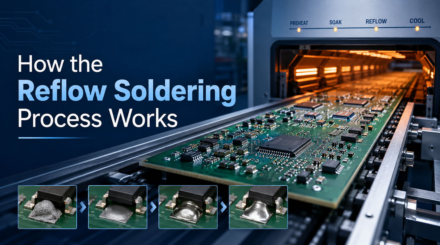
Standard lead-free profile:
- Soak: 60-90 seconds at 150-180°C
- Time Above Liquidus (TAL): 45-60 seconds
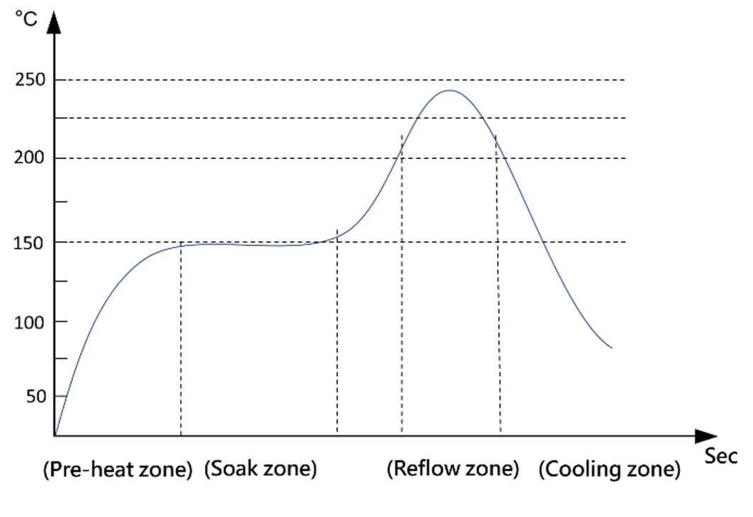
For 2.0mm board with 3550 resistors, this fails. Board acts like heat sink.
Our optimized profile:
- Extended soak: 120 seconds at 160°C
- TAL: 75 seconds at 235°C peak
- Cooling rate: 2.5°C/sec (slow to reduce stressing)
Why? The 2.0mm board needs 40% more time to reach thermal equilibrium. Insufficient soak = temperature gradient across board = cold joints on outer edges.
Thermal Camera Data
| Board Zone | Standard Profile | Optimized Profile | ΔT |
|---|
| Center | 235°C | 237°C | +2°C |
| Edge | 201°C | 231°C | +30°C |
| Resistor pad | 215°C | 234°C | +19°C |
Edge temperature jumped from 201°C to 231°C. That’s the difference between a cold joint and a good joint.
(L.Wang, our process engineer, argued for 140 second soak. We compromised at 120. He was probably right—board still showed 5°C gradient. Added 15 seconds on next batch.)
FR-4 thermal conductivity: 0.3 W/mK. Copper: 398 W/mK. Vias are thermal highways through the board.
Design Requirement
- Resistor power: 20W max
- TCR: 25 ppm/°C (Vishay spec)
- Allowed ΔR: 0.1% → Max ΔT: 40°C
- Ambient: 25°C → Max Tj: 65°C
Thermal resistance calculation:
RθJA = (Tj - Ta) / P = (65 - 25) / 20 = 2.0°C/W
Board without vias: RθJA ≈ 45°C/W (estimate from Flotherm simulation)
Each via (0.3mm diameter, 1.6mm long, plated 25μm):
Rθvia = 1 / (k × A) = 1 / (0.4 W/mmK × 0.07 mm²) = 36°C/W per via
Need 25 vias in parallel: 36°C/W ÷ 25 = 1.44°C/W
Add spreading resistance: ~0.5°C/W
Total: 1.94°C/W → meets 2.0°C/W target.
We placed vias in 5×5 grid, 0.5mm pitch, directly under resistor pad. Diameter capped at 0.3mm to prevent solder wicking.
(First design used 0.4mm vias. Solder wicked down 40% of them, starving pads. Changed to 0.3mm, added solder mask plugs. Problem solved.)
We ran the first batch. Since there was no functional test, we used X-Ray inspection for the First Article Inspection (FAI).
The Data:
- Voiding Rate: The X-ray showed an average void area of 12-15%.
Standard: IPC-A-610F stipulates that a void area percentage of less than 30% for BGA balls is considered acceptable.
Reliability Target: For high power cycling, <5% is ideal, but <20% is acceptable. We hit the safe zone without needing expensive vacuum reflow ovens.
- Defects: Zero “Head-in-Pillow” defects. The extended soak worked.
- Cost: The project NRE was ~20% lower than the per-variant pricing model.
- Time: 18 days from file confirm to shipping.
The Failure Nobody Talks About
Batch #3 had 15% of boards show 12% voiding. Root cause: stencil aperture clogged during printing. Operator didn’t catch it for 30 minutes. We added automatic solder paste inspection (SPI) after this. Cost: $2,100 one-time.
(TM’s engineer asked if we could skip X-ray to save money. We refused. No functional test means process validation is mandatory. They understood.)
Low volume doesn’t mean low quality. TM’s 25-unit batches got the same engineering rigor as 10,000-unit runs.
Key lessons:
The “Hammerhead Dyno” shipped on schedule. TM’s customers measure amplifier power with <0.1% uncertainty. That’s what matters.
(Next challenge: TM wants to add a 4Ω variant. We’re checking if the current panel layout has space. Might need 8% bigger panel. Quote pending.)